Differential Buffer, TSMC N5, North/South (vertical) poly orientation
The multi-channel PHY IP for PCI Express 3.1 includes the vendor’s high-speed, high-performance transceiver to meet today’s appli…
Overview
The multi-channel PHY IP for PCI Express 3.1 includes the vendor’s high-speed, high-performance transceiver to meet today’s applications’ demands for higher bandwidth. The PHY provides a cost-effective solution that is designed to meet the needs of today’s high-speed chip-to-chip, board-to-board, and backplane interfaces while being extremely low in power and area.
Using the leading-edge design, analysis, simulation, and measurement techniques, the vendor delivers exceptional signal integrity and jitter performance that exceeds the PCI Express standards electrical specifications. The high-margin, robust PHY architecture tolerates process, voltage and temperature (PVT) manufacturing variations and is implemented with standard CMOS digital process technologies.
The multi-tap transmitter and receiver equalizers, along with the advanced built-in diagnostics and ATE test vectors, enable customers to control, monitor and test for signal integrity without the need for expensive test equipment. This provides on-chip visibility into actual link and channel performance to quickly improve signal integrity. This capability reduces both product development cycles and the need for costly field support.
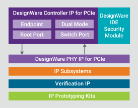
The vendor offers a portfolio of silicon-proven IP for PCI Express consisting of controllers, PHYs, verification IP, IP Prototyping Kits, Software Development Kits and Interface IP Subsystems. As the industry standard for PCI Express, the vendor's solution is in volume production and has been successfully implemented in a wide range of applications.
Key features
- Compliant with the PCI Express (PCIe®) 3.1, 2.1, 1.1 and PIPE specifications
- x1, x2, x4, x8, x16 lane configurations with bifurcation
- Multi-tap adaptive and programmable Continuous Time Linear Equalizer (CTLE) and Decision Feedback Equalization (DFE)
- L1 substate and SRIS support
- Power gating and power island
- Embedded Bit Error Rate (BER) tester and internal eye monitor
- Build-in Self Test vectors, PRBS generation and checker
- IEEE 1149. 6 AC JTAG Boundry Scan
- Supports -40C to 125C junctions
- Supports optional wirebond and flip-chip packaging
Block Diagram
Specifications
Identity
Files
Note: some files may require an NDA depending on provider policy.
Provider
Learn more about Analog IP core
Showcasing AI-Driven Analog Design Migration at Samsung SAFE Forum
What's Driving the World's First Analog and Mixed-Signal Emulation Technology?
Delivering High Quality Analog Video Signals With Optimized Video DACs
Time for multimedia SoCs to get their analog signals right
Scalable Architectures for Analog IP on Advanced Process Nodes
Frequently asked questions about Analog I/O Pad Library IP cores
What is Differential Buffer, TSMC N5, North/South (vertical) poly orientation?
Differential Buffer, TSMC N5, North/South (vertical) poly orientation is a Analog IP core from Synopsys, Inc. listed on Semi IP Hub.
How should engineers evaluate this Analog?
Engineers should review the overview, key features, supported foundries and nodes, maturity, deliverables, and provider information before shortlisting this Analog IP.
Can this semiconductor IP be compared with similar products?
Yes. Buyers can compare this product with similar semiconductor IP cores or IP families based on category, provider, process options, and structured technical specifications.