Overview
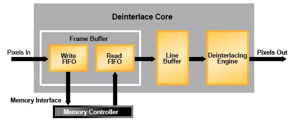
The Deinterlacer IP core converts input video stream from interlaced format into progressive format and uses bob, intra and inter motion adaptive deinterlacing algorithms to reduce interline flicker and jagged edge. The Deinterlacer IP core supports YCbCr4:2:2, YCbCr4:4:4 and RGB format, serial and parallel deinterlacing. The Deinterlacer IP core provides a parameter bus for dynamic parameters updating and the parameter bus can be configured running at a separate clock. Also it supports a simple frame rate conversion function.
Interlaced video frames consists of two sequent fields, which are scanned at even and odd lines of the image sensor. Interlaced video has less transmission bandwidth, but most modern displays support progressive frame only. The two interlaced fields must be converted to one progressive frame for display, which is known as deinterlacing. As the two interlaced fields are taken at different time, there will be flicker and jagged edges in the combined frame. A good deinterlacing algorithm should reduce these artifacts as much as possible and provide good video quality in the process. Lattice Deinterlacer IP core provides several deinterlacing algorithms for different video quality and resource: weave, bob, intra and inter motion adaptive deinterlacing algorithms.
Learn more about Video Processing IP core
Lattice Prompt pairs with AI agentic tools developers already use, combining them with Lattice design tools, knowledge base, and documentation to turn natural language inputs into validated responses, dramatically accelerating FPGA development while optimizing design performance and capability.
First announced on May 4, 2026, the acquisition creates the industry's most complete secure management and control platform.
The acquisition brings together Lattice’s industry-leading low power FPGAs with AMI’s industry‑leading platform firmware and infrastructure manageability solutions for cloud and AI to create a complete portfolio of secure management and control solutions.
The collaboration demonstrates a real-time AI sensor fusion architecture that integrates TI mmWave radar and camera sensors using NVIDIA Holoscan Sensor Bridge running on Lattice’s low power FPGA. The FPGA acts as a companion chip delivering synchronized sensor data directly into GPU-accessible memory to enable low-latency and robust perception for robotics and industrial edge AI applications.
Sets new standard for secure control FPGAs with full CNSA 2.0-compliant post-quantum cryptography, crypto-agility, and hardware Root of Trust for next-generation infrastructure
Lattice Semiconductor today announced that the company expanded its small FPGA portfolio with new, high I/O density options in the Lattice Certus™-NX FPGA and Lattice MachXO5™-NX FPGA device families.