Vendor: Lattice Semiconductor Corp. Category: DDR

DDR3 PHY

The Lattice Double Data Rate (DDR3) Physical Interface (PHY) IP is a general-purpose IP that provides connectivity between a DDR3…

Controller + PHY + 1 DDR3 View all specifications

Overview

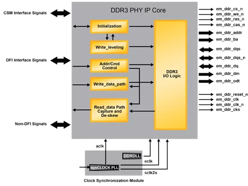
The Lattice Double Data Rate (DDR3) Physical Interface (PHY) IP is a general-purpose IP that provides connectivity between a DDR3 memory Controller (MC) and the DDR3 memory devices compliant with JESD79-3 specification. The DDR3 PHY IP provides the Industry standard DDR PHY Interface (DFI) bus at the local side to interface with the Memory Controller. The DFI protocol defines the signals, signal relationships, and timing parameters required to transfer control information and data to and from the DDDR3 devices over the DFI bus.

The DDR3 PHY IP reduces the effort required to integrate any DDR3 memory controller with Lattice FPGA’s DDR3 primitives and thereby enables the user to implement only the logical portion of the memory controller in the user design. The Lattice’s DDR3 PHY IP contains all the logics required for Memory device initialization procedure, Write leveling, Read data capture and Read data de-skew that are dependent on FPGA DDR IO primitives.

Key features

  • Supports write leveling for each DQS group. Option to switch off write leveling for On-board memory applications
  • Supports all valid DDR3 commands
  • Supports dynamic On-Die Termination (ODT) controls
  • LatticeECP3 I/O primitives manage read skews (Read Leveling equivalent)
  • Option for controlling memory reset outside the IP core
  • 1:1 frequency ratio interface between MC and DFI, 1:2 ratio between DFI and PHY
  • Interfaces to any DDR3 Memory Controller (MC) through DDR PHY Interface (DFI) industry specification
  • Interfaces to industry standard DDR3 SDRAM components and modules compliant with JESD79-3 specification
  • Support for all LatticeECP3 “EA” devices
  • High-Performance DDR3 operations up to 400 MHz/800 Mbps
  • Supports memory data path widths of -8, -16, -24, -32, -40, -48, -56, -64 and -72 bits
  • Supports x4, x8, and x16 device configurations
  • Supports one unbuffered DDR3 DIMM or DDR3 RDIMM module with up to two ranks per DIMM
  • Supports on-board memory (up to two chip selects)
  • Programmable burst lengths of 8 (fixed), chopped 4 or 8 (on-the-fly), or chopped 4 (fixed)
  • Supports automatic DDR3 SDRAM initialization with user mode register programming

Block Diagram

Specifications

Identity

Part Number
DDR3-PHY
Vendor
Lattice Semiconductor Corp.
Type
Silicon IP
Controller / PHY
Controller + PHY , PHY

Standards & Interfaces

Memory
DDR3

Files

Note: some files may require an NDA depending on provider policy.

Provider

Learn more about DDR IP core

DDR3 memory interface controller IP speeds data processing applications

In order to fully capitalize on the benefits of DDR3 memories, it is important to have an efficient and easy to use DDR3 memory interface controller. A video processing application provides a good example of the key requirements of a DDR3 memory system and the features needed from a DDR3 Interface in similar stream-oriented data processing systems.

Microcontroller Design in FPGAs

The union of Microcontroller Unit (MCU) intellectual property (IP) cores with FPGAs provides a far more flexible hardware platform than traditional MCU ASSPs.

Frequently asked questions about DDR Interface IP

What is DDR3 PHY?

DDR3 PHY is a DDR IP core from Lattice Semiconductor Corp. listed on Semi IP Hub.

How should engineers evaluate this DDR?

Engineers should review the overview, key features, supported foundries and nodes, maturity, deliverables, and provider information before shortlisting this DDR IP.

Can this semiconductor IP be compared with similar products?

Yes. Buyers can compare this product with similar semiconductor IP cores or IP families based on category, provider, process options, and structured technical specifications.

×
Semiconductor IP