CXL 3.1 Controller
The Compute Express Link® (CXL®) 3.1 Controller is a parameterizable design for ASIC and FPGA implementations.
Overview
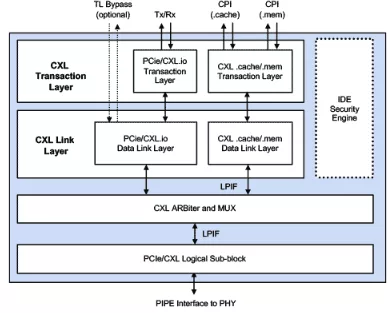
The Compute Express Link® (CXL®) 3.1 Controller is a parameterizable design for ASIC and FPGA implementations. It leverages the Rambus PCIe 6.1 Controller architecture for the CXL.io protocol and adds the CXL.cache and CXL.mem protocols specific to CXL. The controller exposes a native Tx/Rx user interface for CXL.io traffic as well as an Intel CXL-cache/mem Protocol Interface (CPI) for CXL.mem and CXL.
How the CXL 3.1 Controller Works
The controller supports the CXL 3.1 specification and is backward compatible with CXL 2.0 and CXL 1.1. It complies with the Intel PHY Interface for PCI Express (PIPE) specification version 6.x. The provided Graphical User Interface (GUI) Wizard allows designers to tailor the IP to their exact requirements, by enabling, disabling, and adjusting a vast array of parameters. This includes CXL device type, PIPE interface configuration, buffer sizes and latency, low power support, SR-IOV parameters, etc. For optimal throughput, latency, size and power.
The controller can be delivered standalone or integrated with the customer’s choice of CXL 3/PCIe 6 PIPE compliant SerDes. It can also be provided with example reference designs for integration with FPGA SerDes.
Key features
- CXL Layer
- Implements the CXL.io, CXL.mem, and CXL.cache protocols
- Supports all three defined CXL device types
- Supports the PCI Express 6.1 base specification
- Supports the PIPE 6.x specification with 8-, 16-, 32-, 64- and 128-bit configurable PIPE interface width
- Supports operation at x16, x8, x4, x2, x1
- Supports Host, Device, Switch ports and Dual Mode/shared silicon
- Supports Low-latency CXL.mem flit encoder/decoder
- Supports Viral error containment
- Supports deferrable writes
- Supports Standard Intel CPI interface for CXL.mem and CXL.cache
- Supports Sync header bypass and drift buffer modes
- Supports All low-power states
- Supports CXL RAS features (including Viral and Data Poisoning)
- Supports CXL.mem peer to peer and extended metadata feature
- Supports Hot-Plug
- Supports Alternate Protocol Negotiation
- Supports RCiEP
- Supports Global FAM (G-FAM) for Type 3 Device
- Supports Back Invalidation
- Supports lopt low-latency mode
- Supports full datapath parity protection for CXL cache and CXL.mem
- User Interface Layer (Base Version)
- Native 256/512/1024-bit transmit/receive low-latency interface for CXL.io traffic
- Intel-defined CXL-cache/mem Protocol Interface (CPI) for CXL.mem and CXL.cache traffic
- Supports multiple messages in the same clock for both CXL.cache and CXL.mem for both transmit and receive
- User-selectable Transaction/Application Layer clock frequency
- Dedicated sideband interface for Reliability, Availability and Serviceability (RAS) features
- AMBA AXI Layer for CXL.io (AXI Version)
- Compliant with the AMBA AXI Protocol Specification (AXI3, AXI4 and AXI4-Lite)
- Optional AXI4-Lite Subordinate interface for Bridge Configuration
- Optional AXI4-Lite Manager interface for External Registers
- Optional AXI4 Manager Descriptor interface to access SG-DMA Descriptors in AXI domain
- Up to 4 AXI4 Manager interfaces, each supporting up to 128 outstanding read requests
- Up to 4 AXI4 Subordinate interfaces, each supporting up to 512 outstanding read requests
- 64-bit, 128-bit, 256-bit, 512-bit, or 1024-bit data support for AXI4 Manager and Subordinate
- Bypassable CDC for AXI4 Manager and Subordinate
- AXI4 Manager and Subordinate interfaces can be configured as AXI3 interfaces
- Optional built-in Legacy DMA engine
- Up to 8 DMA channels, Scatter-Gather, descriptor prefetch
- Completion reordering, interrupt and descriptor reporting
- Optional Address Translation tables for direct PCIe-to-AXI and AXI-to-PCIe communication
- Integrity and Data Encryption (IDE)
- Implements the CXL 3.1 IDE spec. for CXL.cache/mem
- AES-GCM security supports CXL.mem/CXL.cache at full line rate and with zero latency
- AES-GCM security IP supports PCIe/CXL.io to near full line rate with low latency
- Implements the PCI Express IDE ECN for CXL.io
- Supports containment and skid modes
- Supports early MAC termination
- Supports multi-stream
- Configurable IDE engine
- Supports x1 to x16 lanes
- 256-bit, 512-bit or 1024-bit data bus for PCIe IDE
- 256-bit, 512-bit or 1024-bit data bus for CXL.cache/mem IDE
- High-performance AES-GCM for encrypt, decrypt, authentication
- PCIe IDE TLP aggregation for 1, 2, 4, 8 TLPs
- PCIe IDE automatic IDE prefix insertion and detection
- PCIe IDE automatic IDE sync/fail message generation
- PCRC calculation and validation
- Efficient key control/refresh
- Bypass mode
Block Diagram
Benefits
- Ultra-low Transmit and Receive latency
- Internal data path size automatically scales up or down (256, 512 or 1024 bits) based on max. link speed and width for optimal throughput
- Supports backwards compatibility to PCIe 6.1
- Optional MSI/MSI-X register remapping to memory for reduced gate count when SR-IOV is implemented
- Optional QuickBoot mode allows for up to 4x faster link training, cutting system-level simulation time by 20%
- Loopback Mode support at DLL for CXL.mem and CXL.cache protocols
- Merged Replay and Transmit buffer enables lower memory footprint
- RAS feature support beyond CXLspecification
- Architected to support ASIC and FPGA implementation with the same code base
What’s Included?
- IP Files
- Verilog RTL source code
- Libraries for functional simulation
- Configuration assistant GUI (Wizard)
- Full Documentation
- Reference Designs
- Synthesizable Verilog RTL source code
- Simulation environment and test scripts
- Synthesis project and DC constraint files
- FPGA reference design
Specifications
Identity
Files
Note: some files may require an NDA depending on provider policy.
Provider
Learn more about CXL IP core
Rambus Demonstrates Advancing Data Center Capabilities with CXL Over Optics
Rambus CXL IP: A Journey from Spec to Compliance
New CXL 3.1 Controller IP for Next-Generation Data Centers
CXL 3.1: What's Next for CXL-based Memory in the Data Center
CXL 3.0 Turns Up Scalability to 11
Frequently asked questions about CXL IP cores
What is CXL 3.1 Controller?
CXL 3.1 Controller is a CXL IP core from Rambus, Inc. listed on Semi IP Hub.
How should engineers evaluate this CXL?
Engineers should review the overview, key features, supported foundries and nodes, maturity, deliverables, and provider information before shortlisting this CXL IP.
Can this semiconductor IP be compared with similar products?
Yes. Buyers can compare this product with similar semiconductor IP cores or IP families based on category, provider, process options, and structured technical specifications.