Vendor: Rambus, Inc. Category: CXL

CXL 2.0 Controller

The Compute Express Link™ (CXL™) 2.0 Controller (formerly XpressLINK) leverages a silicon-proven PCIe 5.0 controller architecture…

Overview

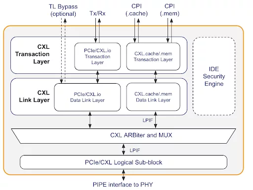
The Compute Express Link™ (CXL™) 2.0 Controller (formerly XpressLINK) leverages a silicon-proven PCIe 5.0 controller architecture for the CXL.io path, and adds CXL.cache and CXL.mem paths specific to the CXL standard. The controller exposes a native Tx/Rx user interface for CXL.io traffic as well as an Intel CXL-cache/mem Protocol Interface (CPI) for CXL.mem and CXL.cache traffic. There is also an CXL 2.0 Controller with AXI version (formerly XpressLINK-SOC) for ASIC and FPGA implementations with support for the AMBA AXI protocol specification for CXL.io and either CPI or AXI for CXL.mem, and CPI for CXL.cache or the AMBA CXS-B protocol specification.

How the CXL 2.0 Controller Works

The controller supports the CXL 2.0 specification and is backward compatible with CXL 1.1. It complies with the Intel PHY Interface for PCI Express (PIPE) specification version 5.x. The provided Graphical User Interface (GUI) Wizard allows designers to tailor the IP to their exact requirements, by enabling, disabling, and adjusting a vast array of parameters, including CXL device type, PIPE interface configuration, buffer sizes and latency, low power support, SR-IOV parameters, etc. for optimal throughput, latency, size and power. The controller has been extensively verified using commercial and internally developed VIP and test suites. It can be paired with a number of 3rd-party CXL PHYs.

The CXL 2.0 controller has been extensively verified using commercial and internally developed VIP and test suites.

Key features

  • CXL Protocol Layer
    • Comprises complete CXL 2.0 interconnect subsystem with Rambus CXL 2.0 PHY
    • Supports the CXL 2.0 specification; backward compatible with CXL 1.1
    • Implements the CXL.io, CXL.mem, and CXL.cache protocols
    • Supports all 3 defined CXL device types
    • Supports Host, Device, Switch ports and Dual Mode/shared silicon implementation
    • Supports the PCI Express 5.0 base specification revision 1.0
    • Supports the PIPE 5.x specification with 8, 16, 32, 64 and 128-bit configurable PIPE interface width
    • Supports CXL device configurations
    • Supports operation at x16, x8, x4, x2, x1
    • Compliant with PCI-SIG Single-Root I/O Virtualization (SR-IOV) Specification
    • Supports up to 64 Physical Functions (PF), 512 Virtual Functions (VF)
    • Supports PCI Express Advanced Error Reporting (AER)
    • Supports optional ECNs
    • Supports Port Bifurcation
    • Supports deferrable writes
    • Supports DOE, CMA over DOE
  • User Interface Layer
    • PLDA native 256/512-bit transmit/receive low-latency interface for CXL.io traffic
    • Intel-defined CXL cache/mem Protocol Interface (CPI) for CXL.mem and CXL.cache traffic
    • User-selectable Transaction/Application Layer clock frequency (CXL.io)
    • Dedicated sideband interface for Reliability, Availability and Serviceability (RAS) features
  • Integrity and Data Encryption (IDE)
    • AES-GCM security supports CXL.mem/CXL.cache at full line rate and with zero latency
    • AES-GCM security IP supports PCIe/CXL.io to near full line rate with low latency
    • Implements the CXL 2.0 IDE specifications for CXL.cache/mem
    • Implements the PCI Express IDE ECN for CXL.io
    • Configurable IDE engine
    • Supports x1 to x16 lanes
    • Supports all device types
    • 256-bit or 512-bit data bus for PCIe IDE
    • 512-bit data bus for CXL.cache/mem IDE
    • Supports containment and skid modes
    • Supports early MAC termination
    • Supports multi-stream
    • Utilizes high-performance AES-GCM for encryption, decryption, authentication
    • PCIe IDE TLP aggregation for 1, 2, 4, 8 TLPs
    • PCIe IDE automatic IDE prefix insertion and detection
    • PCIe IDE automatic IDE sync/fail message generation
    • PCRC calculation & validation
    • Efficient key control/refresh
    • Bypass mode

Block Diagram

Benefits

  • Internal data path size automatically scales up or down (256-, 512- bits) based on max. link speed and width for reduced gate count and optimal throughput
  • Dynamically adjustable application layer frequency down to 8Mhz for increased power savings
  • Optional MSI/MSI-X register remapping to memory for reduced gate count when SR-IOV is implemented
  • Configurable pipelining enables full speed operation on Intel and Xilinx FPGA, full support for production FPGA designs (when supported)
  • Ultra-low Transmit and Receive latency
  • Smart buffer management on receive side (Rx Stream) allows implementation of custom credit management schemes in the application logic
  • Merged Replay and Transmit buffer enables lower memory footprint
  • Optional Transaction Layer bypass allows for customer specific transaction layer and application layer
  • Optional QuickBoot mode allows for up to 4x faster link training, cutting system-level simulation time by 20%

Applications

  • HPC,
  • Cloud Computing,
  • AI,
  • Machine Learning,
  • Enterprise,
  • Networking,
  • Automotive,
  • AR/VR,
  • Test and Measurement

What’s Included?

  • Verilog RTL,
  • Supporting Documentation

Specifications

Identity

Part Number
CXL 2.0 Controller
Vendor
Rambus, Inc.
Type
Silicon IP

Videos

Demonstration of a CXL Interconnect on a FPGA-based design
In this video, we demonstrate the Rambus Controller IP for CXL 2.0 and the CXL.mem protocol used to access Host-managed Device Memory, or HDM. This demonstration is performed using Intel’s Pre-Production Xeon processor as a host, connected to an FPGA board, instantiating Rambus' CXL Controller and CXL.mem test design.

Files

Note: some files may require an NDA depending on provider policy.

Provider

HQ: USA

Learn more about CXL IP core

Rambus CXL IP: A Journey from Spec to Compliance

[Updated April 7, 2025] With the ongoing efforts of the Rambus engineering team, we have now achieved compliance to CXL 2.0 with our CXL Controller IP, and it has been added to the Integrators List.

Frequently asked questions about CXL IP cores

What is CXL 2.0 Controller?

CXL 2.0 Controller is a CXL IP core from Rambus, Inc. listed on Semi IP Hub.

How should engineers evaluate this CXL?

Engineers should review the overview, key features, supported foundries and nodes, maturity, deliverables, and provider information before shortlisting this CXL IP.

Can this semiconductor IP be compared with similar products?

Yes. Buyers can compare this product with similar semiconductor IP cores or IP families based on category, provider, process options, and structured technical specifications.

×
Semiconductor IP