Overview
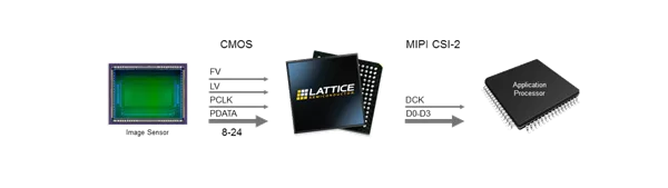
Many traditional image sensors have a CMOS interface. However, many mobile applications processors only have MIPI CSI-2 interfaces. Many new applications want to leverage mobile innovations, while utilizing traditional image sensors with specific requirements and capabilities.
Lattice CrossLink™ is a programmable video interface bridging device capable of converting image sensors with CMOS interfaces up to 300 MHz to MIPI CSI-2 interfaces at up to 6 Gbps. This bridge is available as free IP in Lattice Diamond® for allowing easy configuration and setup.
Features * Supports MIPI DSI and MIPI CSI-2 outputs up to 6 Gbps: 1, 2 or 4 data lanes
* Supports parallel MIPI DPI, CMOS, RAW and RGB interfaces at up to 300 MHz
* Supports CSI-2 compatible video formats (RAW, RGB, and YUV): * 8-bit YUV420/422
* 10-bit YUV420/422
* 8-bit RAW8
* 10-bit RAW10
* 12-bit RAW12
* 24-bit RGB888
* Supports DSI compatible video formats (RGB) : * 18-bit RGB666
* 24-bit RGB888
* Supports multiple pixels per clock mode * 10, 8, 6, 4, and 1 for RAW8/10/12
* 4, 2, and 1 for RGB888/666
* Provides a DCS (Display Command Set) controller to program the display, ROM data used only for DSI in HS or LPDT mode – ROM is programmable by user
* Configurable 2-bit VC (Virtual Channel), 6-bit DT (Data Type), and 16-bit WC (Word Count)
* Supports Non-burst Mode with Sync Events for Transmission Packet Sequence
* Compliance with MIPI D-PHY Specification v1.1
* Compliance with DSI and CSI-2 Specification v1.1
Learn more about MIPI IP core
Extending Lattice's post-quantum cryptography leadership from silicon to a complete platform security stack, Lattice Sentry now delivers CNSA 2.0-aligned, NIST-compliant protection across AI data centers, and critical infrastructure, giving system designers a validated, production-ready path to quantum-resistant security.
Combining Arm® AGI CPU server platforms with Lattice FPGAs and AMI firmware creates a solution that provides advanced security, manageability, connectivity, and flexibility for next-generation AI data center infrastructure.
Lattice Prompt pairs with AI agentic tools developers already use, combining them with Lattice design tools, knowledge base, and documentation to turn natural language inputs into validated responses, dramatically accelerating FPGA development while optimizing design performance and capability.
First announced on May 4, 2026, the acquisition creates the industry's most complete secure management and control platform.
The acquisition brings together Lattice’s industry-leading low power FPGAs with AMI’s industry‑leading platform firmware and infrastructure manageability solutions for cloud and AI to create a complete portfolio of secure management and control solutions.
The collaboration demonstrates a real-time AI sensor fusion architecture that integrates TI mmWave radar and camera sensors using NVIDIA Holoscan Sensor Bridge running on Lattice’s low power FPGA. The FPGA acts as a companion chip delivering synchronized sensor data directly into GPU-accessible memory to enable low-latency and robust perception for robotics and industrial edge AI applications.