Vendor: Cadence Design Systems, Inc. Category: UltraLink

40G UltraLink D2D PHY

High-performance, low-latency PHY for D2D connectivity

GlobalFoundries 12nm LP Silicon Proven View all specifications

Overview

High-performance, low-latency PHY for D2D connectivity

The Cadence UltraLink™ Die-to-Die (D2D) PHY enables SoC providers to deliver more customized solutions that offer higher performance and yields while also shortening development cycles and reducing costs through greater IP reuse.

It is a mature solution that is silicon proven in multiple foundries and different process nodes.

Key features

  • Innovative mixed-signal architecture to achieve high bandwidth, ultra low latency and low power 
  • Flexible data rate from 20Gbps to 40Gbps 
  • Built-in self-test features to ensure “known good die” 
  • Interoperable between different technology nodes and foundries 
  • Easy routing and straightforward integration 
  • Achieves better than 10-15 bit error rate (BER) without requiring forward error correction (FEC) 
  • Integrated scrambling and lane de-skew functionality 
  • Supports -40ºC to 125ºC industrial temperature range 

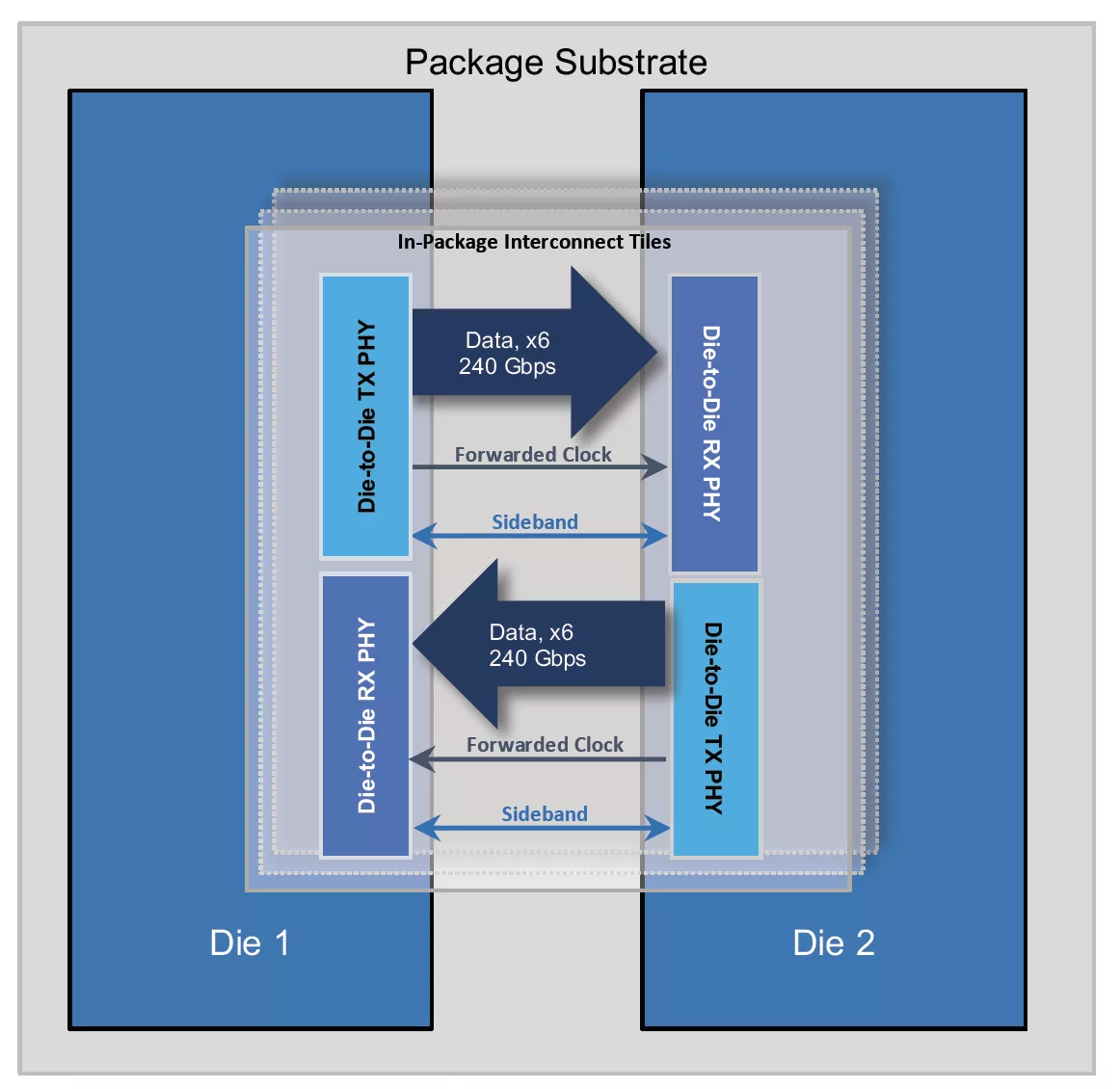
Block Diagram

Benefits

  • Ultra-Low Latency: Optimized for latency-sensitive applications
  • High Performance: 40Gbps wire speed delivers up to 1Tbps/mm unidirectional bandwidth
  • Cost Effective: Supports multi-chip module on organic substrates

Silicon Options

Foundry Node Process Maturity
GlobalFoundries 12nm LP Silicon Proven

Specifications

Identity

Part Number
40G UltraLink D2D PHY
Vendor
Cadence Design Systems, Inc.
Type
Silicon IP

Files

Note: some files may require an NDA depending on provider policy.

Provider

Learn more about UltraLink IP core

Cadence Expands Sovereign AI in Europe: From Chips to AI Factories

To bring computing scale and regional data control together, Cadence is expanding its sovereign AI data center in Munich, becoming the first electronic design automation (EDA)opens in a new tab vendor to deliver a comprehensive sovereign AI platform for semiconductor, system, and AI factory design in Europe.

The Memory Challenge of Physical AI

As physical AI workloads become more complex, architects must now consider how predictably the complete system performs when multiple real-world workloads are active simultaneously.

PCI Express Security and TEE Integration, Part 1 - Establishing Trust

Protecting processor memory alone is no longer sufficient. The entire I/O path must become part of the trusted computing architecture. To address this challenge, PCI-SIG® has developed a suite of complementary security technologies, including Data Object Exchange (DOE), Component Measurement and Authentication (CMA), Integrity and Data Encryption (IDE), and the TEE Device Interface Security Protocol (TDISP).

Frequently asked questions about UltraLink IP cores

What is 40G UltraLink D2D PHY?

40G UltraLink D2D PHY is a UltraLink IP core from Cadence Design Systems, Inc. listed on Semi IP Hub. It is listed with support for globalfoundries Silicon Proven.

How should engineers evaluate this UltraLink?

Engineers should review the overview, key features, supported foundries and nodes, maturity, deliverables, and provider information before shortlisting this UltraLink IP.

Can this semiconductor IP be compared with similar products?

Yes. Buyers can compare this product with similar semiconductor IP cores or IP families based on category, provider, process options, and structured technical specifications.

×
Semiconductor IP