12-bit, 2.5Msps, 3V, 0.4µs, SAR Analog-to-Digital Converter IP
12-bit, 2.5Msps, 3V, 0.4µs, successive approximation register (SAR) analog-to-digital converter (A/D) that is fabricated using TSMC's CLN40LP
Overview
The AT40LADC000112206BSAA1 is a 12-bit, 2.5Msps, 3V, 0.4µs, successive approximation register (SAR) analog-to-digital converter (A/D) that is fabricated using TSMC's CLN40LP (CMOS Logic Node 40nm Low Power (LP)) process technology.
Electrical characteristics
| Item | Unit | Spec MIN | Spec TYP | Spec MAX | Description |
|---|---|---|---|---|---|
| Analog operating voltage (VCCA) | V | 2.7 | 3.3 | 3.6 | |
| Digital operating voltage (VDD) | V | 1.04 | 1.2 | 1.26 | |
| Reference voltage (VREF) | V | 2.7 | 3.3 | 3.6 | VCCA ≥ VREF |
| Junction temperature (Tj) | °C | -40 | 25 | 125 | |
| Resolution | bits | 8 | 10 | 12 | selectable |
| Clock frequency (ADCLK) | MHz | - | 60 | 61.5 | |
| Analog input range (Vin) | V | 0 | VREF | Single ended | |
| Analog input channel number | n | - | - | 1 | No multiplexer included |
| Conversion rate (Fconv) | Msps | - | - | 2.5 | ADCLK=60MHz, 12bit |
| Conversion time (Tconv) | µs | 0.4 | - | - | ADCLK=60MHz, 12bit |
| Integral Non-Linearity (INL) | LSB | -2 | - | +2 | 12bit |
| Differential Non-Linearity (DNL) | LSB | -1 | - | +1 | 12bit |
| Absolute accuracy (Abs) | LSB | -4 | - | +4 | 12bit |
| Power consumption (Icc) | mA | - | 0.7 | 1.1 | ADCLK=60MHz, VCCA pin |
Key features
- Conversion method: Successive approximation
- Resolution: 12/10/8-bit selectable
- Conversion time: 0.4μs
- Differential nonlinearity (DNL): -1LSB(Min.)/+1LSB(Max.)
- Integral nonlinearity (INL): -2LSB(Min.)/+2LSB(Max.)
- Supply voltage: VCCA = 2.7V to 3.6V
- Analog input range: 0 to VREF, single-ended, no multiplexer included
- Process: TSMC CLN40LP
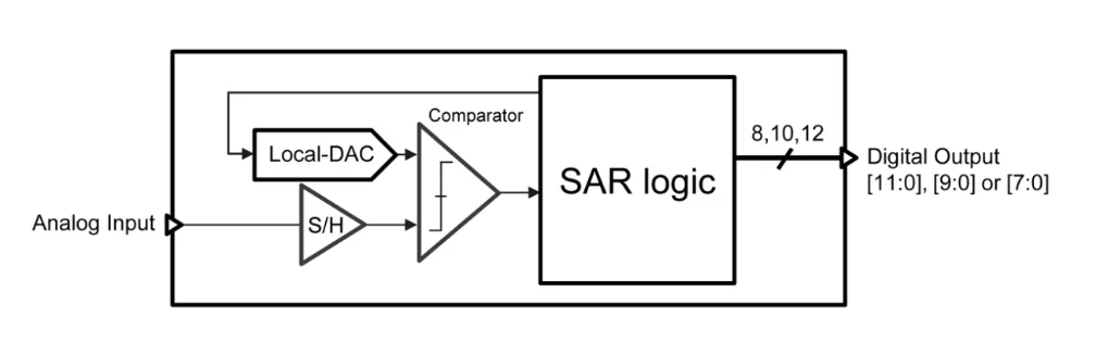
Block Diagram
Silicon Options
| Foundry | Node | Process | Maturity |
|---|---|---|---|
| TSMC | 40nm | LP eFlash | Available on request |
Specifications
Identity
Analog
Files
Note: some files may require an NDA depending on provider policy.
Provider
Learn more about ADC IP core
Renesas Develops 3nm TCAM Technology Combining High Memory Density and Low Power, Suitable for Automotive SoCs
Renesas Partners with Indian Government to Drive Innovation Through Startups and Industry-Academia Collaboration, Strengthening India’s Semiconductor Ecosystem
Renesas Completes Acquisition of Altium
Industry's First General-Purpose 32-bit RISC-V MCU Core Expands Design Freedom
Renesas Introduces Industry's First General-Purpose 32-bit RISC-V MCUs with Internally Developed CPU Core
Frequently asked questions about ADC IP cores
What is 12-bit, 2.5Msps, 3V, 0.4µs, SAR Analog-to-Digital Converter IP?
12-bit, 2.5Msps, 3V, 0.4µs, SAR Analog-to-Digital Converter IP is a ADC IP core from Renesas listed on Semi IP Hub. It is listed with support for tsmc Available on request.
How should engineers evaluate this ADC?
Engineers should review the overview, key features, supported foundries and nodes, maturity, deliverables, and provider information before shortlisting this ADC IP.
Can this semiconductor IP be compared with similar products?
Yes. Buyers can compare this product with similar semiconductor IP cores or IP families based on category, provider, process options, and structured technical specifications.