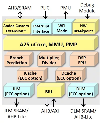
AndesCore™ A25 is a 32-bit CPU IP core based on AndeStar™ V5 architecture which incorporated RISC-V technology, it is capable of delivering high per-MHz performance and operating at high frequencies, at the same time it is small in gate count. A25 also supports the RISC-V P-extension (draft) DSP/SIMD ISA contributed by Andes, single- and double-precision floating point and bit-manipulation instructions, and MMU for Linux based applications. A25 comes with options, including branch prediction for efficient branch execution, Instruction and Data caches, Local Memories for low-latency accesses, ECC for L1 memory soft error protection, and Andes Custom Extension™ (ACE) to add proprietary instructions to accelerate performance/power consumption critical spots.
A25’s 5-stage pipeline is optimized for high operating frequency and high performance. Features also includes PLIC and vectored interrupts for serving various types of system events, AXI 64-bit or AHB 64/32-bit bus, PowerBrake, QuickNap™ and WFI mode for low power and power management, and JTAG debug interface for development support.
Development Tools
- AndeSight™ Integrated Development Environment
- COPILOT: Custom-OPtimized Instruction deveLOpment Tool for ACE
- ICE debugging hardware
Key Features and Performance
AndeStar™ V5 Architecture
| Key Features |
Benefits |
| RISC-V RV32IMACFDBP instructions |
- State-of-the art ISA from latest developments in computer architecture
- Industry standard and open architecture
|
| RISC-V single and double precision floating point instruction |
Accelerate the processing of high precision arithmetic |
| RISC-V bit-manipulation instructions, including the Zba, Zbb, Zbc and Zbs extensions |
Benefits codes with bit-wise operations |
| Andes Extended Instructions |
Andes exclusive performance and functionality enhancements |
| Andes Custom Extension™ (ACE) option to create customized instructions for software acceleration |
- Add customized instruction extensions to facilitate Domain-Specific Architecture/Acceleration (DSA)
- Boost application performance significantly, at the same time maintain the programmability
- Powerful constructs are available to define high level instruction
- ACE design is based on Verilog and C languages which are familiar to the designers
- The COPILOT tool automatically generates the extended CPU and software toolchain
- Do not require expertise in processor pipeline to design ACE instructions
|
| 16/32-bit mixable instruction format |
For compact code density |
| 32 general-purpose registers |
For better code size and performance |
| Machine (M), User (U) and Supervisor (S) Privilege levels |
For Linux and advanced operating systems with protection between kernel and user programs |
CPU Core
| Key Features |
Benefits |
| 3.57 Coremark/MHz, 1.98 DMIPS/MHz* |
Superior performance-per-MHz |
| 5-stage pipeline, with a full-cycle reserved for critical SRAM accesses |
Superior performance-efficiency, while allowing for high speeds |
|
Extensive branch prediction features
- Branch Target Buffer (BTB): 32, 64, 128 or 256-entry
- Branch History Table (BHT): 256-entry, with 8-bit branch history
- Return Address Stack (RAS): 4-entry
|
- Branch Target Buffer and Branch History Table to speed up control codes
- Return Address Stack to speeds up procedure returns
|
|
Memory Management Unit
- Sv32 virtual-memory systems
- 4/8-entry fully associative ITLB/DTLB
- 32/64/128-entry 4-way set-associative shared TLB
- Hardware page table walker
|
- Virtual memory support for full address space and easy code/data sharing
- Support for full-featured OS such as Linux
- Protection of supervisor and user privilege
- Hardware for fast address translation
|
| Physical Memory Protection (PMP), 16 regions |
Basic read/write/execute memory protection with minimum cost |
| Performance monitors |
Program code performance tuning |
| StackSafe™ hardware stack protection |
- Easy identification of stack size threshold during development
- Hardware error detection of stack overflow and underflow at runtime
|
|
Multiplier options
- Fast multiplier: pipelined, 2-cycle
- Small multipliers: producing 1, 2, 4, or 8 bits per cycle
|
Option to choose between speed and area according to application's requirements |
| PowerBrake technology |
Performance throttling to digitally reduce power consumption |
| QuickNap™ technology |
Fast power-down/wake-up support for caches |
* AndeSight v500, DMIPS/MHZ follow Dhrystone’s no-inline ground rules, best performances
Memory Subsystems
| Key Features |
Benefits |
|
I-Cache & D-Cache
- Size: 4KB to 64KB
- Set associativity: Direct-mapped, 2-way or 4-way
|
- Accelerating accesses to slow memories
- Flexible cache configurations
|
|
ILM & DLM
- Size: 4KB to 16MB
- SRAM or AHB-Lite interface support
- Bus manager accesses by local memory access port
|
- For deterministic and efficient program execution
- Flexible size selection to fit diversified needs
|
| Soft-error protection: ECC or parity for I-Cache and D-Cache, ILM and DLM with SRAM interface |
Code and data integrity protection |
| Bus manager port: AHB or AXI with 64-bit data, 32 to 64-bit address, AXI with I/D separate or joint bus |
User-selectable bus interface for optimal efficiency |
| Bus subordinate port: AHB with 64-bit data, for ILM/DLM accesses |
Efficient data transfer between CPU and SoC managers |
| Core/bus clock ratio of N:1 |
Simplified SoC integration |
Platform-Level Interrupt Controller (PLIC)
| Key Features |
Benefits |
|
Implements RISC-V PLIC specification
- Up to 1023 PLIC interrupt sources
- Up to 255 PLIC interrupt priority levels
- Up to 16 PLIC interrupt targets
|
Allow individual interrupts to be serviced and prioritized without sharing |
|
Enhanced interrupt features
- Vectored interrupt dispatch
- Priority-based preemption
- Selectable edge trigger or level trigger
|
- Faster interrupt handling for real-time applications
- Complete hardware preemption support for faster response
- Flexible interrupt source interface for simpler SoC design
|
Debug Support
| Key Features |
Benefits |
| Implements RISC-V debug specifications |
Supported by industry debug tool suppliers |
| JTAG Debug Port |
Industry-standard support |
| Embedded Debug Module with up to 8 triggers |
Flexible configurations to tradeoff between gate count and debugging capabilities |
| Exception redirection support |
Entering debugger upon selected exceptions without using breakpoints |
Performance
| Core, Process |
A25 (w/o DSP, FPU), 28HPC+ |
A25 (with DSP, FPU), 28HPC+ |
| Frequency (MHz) |
1000 |
1000 |
| Dynamic power (uW/MHz) |
17 |
20 |
| Area (mm2) |
0.084 |
0.165 |
* Configured with cache and MMU. SVT 9-track library, SS corner, 0.81V, -40°C, and with I/O constraint. Power consumption at TT corner, 0.9V, 25°C