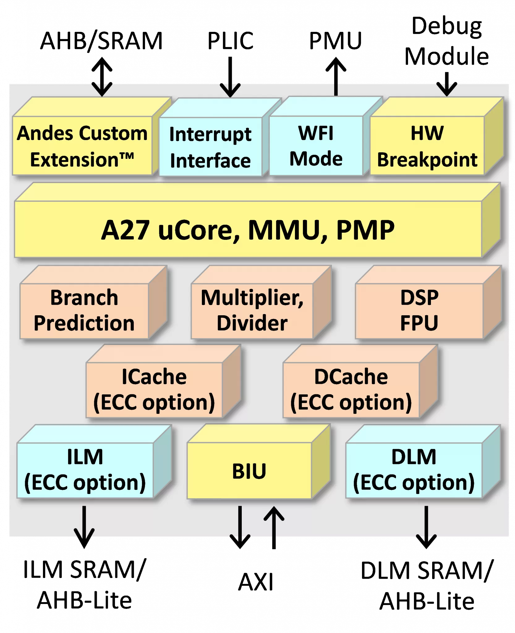
The 32-bit A27 is a 5-stage processor that supports the latest RISC-V specification, including "G" ("IMAFD") standard instructions, "C" 16-bit compression instructions, "P" Packed-SIMD/DSP instructions, "N" for user-level interrupts, and Memory Management Unit (MMU) for Linux support.
A27 features branch prediction, instruction and data caches, local memories, ECC error protection, and Andes Custom Extension™ to add custom instructions to accelerate performance and reduce power consumption. In addition, it incorporates MemBoost to greatly enhance memory bandwidth and reduce memory latencies for applications with intensive memory accesses. A27 also includes vectored and preemptive interrupt controller to serve diversified system events, AXI 64-bit bus, rich power management, and JTAG debug interface and trace interface for software development support.
Development Tools
- AndeSight™ Integrated Development Environment
- COPILOT: Custom-OPtimized Instruction deveLOpment Tool for ACE
- ICE debugging hardware
Key Features and Performance
AndeStar™ V5 Architecture
| Key Features |
Benefits |
| RISC-V RV32GC-N-P ISA |
- State-of-the art ISA from latest developments in computer architecture
- Industry standard and open architecture
|
| RISC-V P-extension (draft) DSP/SIMD instructions with versatile operations |
Boost the performance of voice, audio, image and signal processing |
| RISC-V single and double precision floating point instruction |
Accelerate the processing of high precision arithmetic |
| Andes Extended Instructions |
Andes exclusive performance and functionality enhancements |
| Andes Custom Extension™ (ACE) option to create customized instructions for software acceleration |
- Add customized instruction extensions to facilitate Domain-Specific Architecture/Acceleration (DSA)
- Boost application performance significantly, at the same time maintain the programmability
- Powerful constructs are available to define high level instruction
- ACE design is based on Verilog and C languages which are familiar to the designers
- The COPILOT tool automatically generates the extended CPU and software toolchain
- Do not require expertise in processor pipeline to design ACE instructions
|
| 16/32-bit mixable instruction format |
For compact code density |
| 32 general-purpose registers |
For better code size and performance |
| Machine (M), User (U) and Supervisor (S) Privilege levels |
For Linux and advanced operating systems with protection between kernel and user programs |
CPU Core
| Key Features |
Benefits |
| 3.57 Coremark/MHz, 1.98 DMIPS/MHz* |
Superior performance-per-MHz |
| 5-stage pipeline, with a full-cycle reserved for critical SRAM accesses |
Superior performance-efficiency, while allowing for high speeds |
|
Extensive branch prediction features
- Branch Target Buffer (BTB): 32, 64, 128 or 256-entry
- Branch History Table (BHT): 256-entry, with 8-bit branch history
- Return Address Stack (RAS): 4-entry
|
- Branch Target Buffer and Branch History Table to speed up control codes
- Return Address Stack to speeds up procedure returns
|
|
Memory Management Unit
- Sv32 virtual-memory systems
- 4/8-entry fully associative ITLB/DTLB
- 32/64/128-entry 4-way set-associative shared TLB
- Hardware page table walker
|
- Virtual memory support for full address space and easy code/data sharing
- Support for full-featured OS such as Linux
- Protection of supervisor and user privilege
- Hardware for fast address translation
|
| Physical Memory Protection (PMP), 16 regions |
Basic read/write/execute memory protection with minimum cost |
| Programmable Physical Memory Attribute (PMA), 16 regions |
Configurable memory attributes:
- Memory, I/O, None
- Cacheable/Non-cacheable
- Write-back/Write-through
- Read/write/read & write allocate, no allocate
- Access fault for non-existent regions
|
| Performance monitors |
Program code performance tuning |
| StackSafe™ hardware stack protection |
- Easy identification of stack size threshold during development
- Hardware error detection of stack overflow and underflow at runtime
|
|
Multiplier options
- Fast multiplier: pipelined, 2-cycle
- Small multipliers: producing 1, 2, 4, or 8 bits per cycle
|
Option to choose between speed and area according to application's requirements |
| PowerBrake technology |
Performance throttling to digitally reduce power consumption |
| QuickNap™ technology |
Fast power-down/wake-up support for caches |
* AndeSight v500, DMIPS/MHZ follow Dhrystone’s no-inline ground rules, best performances
Memory Subsystems
| Key Features |
Benefits |
|
I-Cache & D-Cache
- Size: 8KB to 64KB
- Set associativity: 2-way or 4-way
|
- Accelerating accesses to slow memories
- Flexible cache configurations
|
|
ILM & DLM
- Size: 4KB to 16MB
- SRAM or AHB-Lite interface support
- Bus manager accesses by local memory access port
|
- For deterministic and efficient program execution
- Flexible size selection to fit diversified needs
|
| MemBoost – Data Cache Write-Around |
Smart cache line allocation policy, for better cache utilization and reduce number of memory accesses |
| MemBoost – Instruction and Data Pre-fetch |
Conditionally fill instruction and data caches in advance, for minimum memory access latency |
| MemBoost – Multiple Outstanding Mem. Req. |
Issue multiple transactions to data memory sub-system for higher bus utilization, also support out-of-order completion |
| MemBoost – Dedicated I & D Bus Interfaces |
Separate instruction and data buses, for instruction and data's own memory transactions |
| Soft-error protection: ECC or parity for I-Cache and D-Cache, ILM and DLM with SRAM interface |
Code and data integrity protection |
| Bus manager port: AXI with 64/128-bit data, I/D joint or separate bus |
User-selectable bus interface for optimal efficiency |
| Bus subordinate port: AHB with 64/128-bit data, for ILM/DLM accesses |
Efficient data transfer between CPU and SoC managers |
| Core/bus clock ratio of N:1 |
Simplified SoC integration |
Platform-Level Interrupt Controller (PLIC)
| Key Features |
Benefits |
|
Implements RISC-V PLIC specification
- Up to 1023 PLIC interrupt sources
- Up to 255 PLIC interrupt priority levels
- Up to 16 PLIC interrupt targets
|
Allow individual interrupts to be serviced and prioritized without sharing |
|
Enhanced interrupt features
- Vectored interrupt dispatch
- Priority-based preemption
- Selectable edge trigger or level trigger
|
- Faster interrupt handling for real-time applications
- Complete hardware preemption support for faster response
- Flexible interrupt source interface for simpler SoC design
|
Debug Support
| Key Features |
Benefits |
| Implements RISC-V debug specifications |
Supported by industry debug tool suppliers |
| JTAG Debug Port |
Industry-standard support |
| Embedded Debug Module with up to 8 triggers |
Flexible configurations to tradeoff between gate count and debugging capabilities |
| Exception redirection support |
Entering debugger upon selected exceptions without using breakpoints |
Performance
| Core, Process |
A27, 28nm |
| Frequency (MHz) |
1000 |
| Dynamic power (uW/MHz) |
21 |
| Area (mm2) |
0.131 |
* Configured with 32KB instruction and data caches, MMU with 256-entry BTB, 16-entry PMP and 16-entry PMA, without DSP and FPU. Using SVT 9-track library, SS corner, 0.81V, -40°C, and with I/O constraint. Power consumption at TT corner, 0.9V, 25°C