Overview
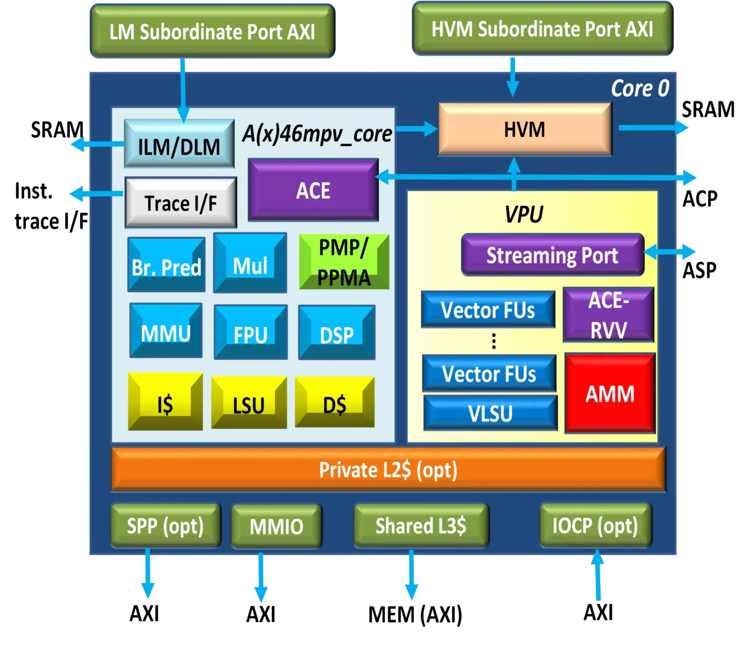
AndesCore™ AX46MP(V) 64-bit multicore CPU IP is an 8-stage superscalar processor with Vector Processing Unit (VPU) based on AndeStar™ V5 architecture and Andes Matrix Multiply (AMM) extension. It supports RISC-V standard “G (IMA-FD)”, “ZC” compression, “B” bit manipulation, DSP/SIMD ‘P’ (draft), “V” (vector), CMO (cache management) extensions, Andes performance enhancements, plus Andes Custom Extension™ (ACE) for user-defined instructions. It supports all RVA22 profile mandatory ISAs. It features MMU for Linux based applications, dynamic branch prediction for efficient branch execution, dual-issue of common instruction pairs, level-1 private instruction/data caches, private level-2 cache and local memories for low-latency accesses. The AX46MP(V) symmetric multiprocessor supports up to 16 cores and a shared level-3 cache controller. Coherence Manger ensures data coherence among CPU accesses and IO transactions from external bus managers. All caches are non-blocking with prefetch support. The AX46MPV have a powerful VPU with up to 2048b VLEN and Matrix unit, is excellent for computations involving large arrays of data.
AndeStar™ V5 Architecture
| Key Features |
Benefits |
RISC-V RV64 GCBPV+CMO
RVA22 Compliant |
- State-of-the art ISA from latest developments in computer architecture
- Industry standard and open architecture
|
| Andes Extended Instructions |
Andes exclusive performance and functionality enhancements |
| MMU and Sv39/Sv48/SV57 virtual memory translation |
For Linux and advanced operating systems with protection between kernel and user program |
| 64-bit CPU architecture with Dynamic UXL (AX46MPV, AX46MP) |
Enabling software to utilize the memory spaces far beyond the 4G byte limit of 32-bit CPUs, while still capable of running 32bit application |
| Machine (M), User (U) and Supervisor (S) Privilege levels |
Full privilege protections |
CPU Core
| Key Features |
Benefits |
| >6.3 CoreMark/MHz, >3.9 DMIPS/MHz, >4.3 SpecInt2006/Ghz |
Superior performance-per-MHz |
| 8-stage in-order superscalar pipeline |
Superior performance-efficiency, while allowing for high speeds |
|
Extensive branch predication features
- Branch Target Buffer (BTB)
- Branch Histroy Table (BHT)
- Return Address Stack (RAS)
|
- Branch Target Buffer and Branch History Table to speed up control codes
- Return Address Stack to speeds up procedure returns
|
|
MMU (Memory Management Unit)
- Sv39, Sv48, SV57 virtual-memory systems
- 4/8-entry fully associative ITLB/DTLB
- 32-512 entry 4-way set-associative shared TLB
- Hardware page table walker
|
- Virtual memory support for full address space and easy code/data sharing
- Support for full-featured OS such as Linux
- Protection of supervisor and user privilege
- Hardware for fast address translation
|
| Physical Memory Protection (PMP), configurable up to 32 regions |
Basic read/write/execute memory protection with minimum cost |
| Programmable Physical Memory Attribute (PMA), configurable up to 16 regions |
Configurable memory attributes:
- Memory, I/O, None
- Cacheable/Non-cacheable
- Read/write/read & write allocate, no allocate
- Access fault for non-existent regions
|
| Performance monitors |
Program code performance tuning |
| StackSafe™ hardware stack protection |
- Easy identification of stack size threshold during development
- Hardware error detection of stack overflow and underflow at runtime
|
| PowerBrake technology |
Performance throttling to digitally reduce power consumption |
* DMIPS/MHZ follow Dhrystone’s no-inline ground rules, best performances
Memory Subsystems
| Key Features |
Benefits |
|
Level-1 I-Cache & D-Cache
- Size: 16KB to 64KB
- Cache line size: 64 bytes
- Set associativity: 4-way
Level-2 Private Unified Cache
- Configurable from 64KB to 512KB
- 64-byte cache line size
- 8-way, pseudo random replacement
Level-3 Shared Cache
- Configurable from 256KB to 32MB
- 64-byte cache line size
- 16-way, pseudo random replacement
|
- Accelerating accesses to slow memories
- Flexible cache configurations
- Accelerate performance with larger private 2nd level cache
- Large shared L3 cache
|
|
ILM & DLM
- Size: 4KB to 16MB
- Scalar core access only
- SRAM interface support
- Bus managers accessed by AXI subordinate port
|
- For deterministic and efficient program execution
- Flexible size selection to fit diversified needs
|
|
HVM
- Size: 32KB to 4GB
- Accessible by both VPU and scalar core
- Fast vector access with DLEN data width
- Subordinate port for external DMA
- When MMU is configured, HVM is addressed by translated physical memory, therefore it can also work with virtual memory under Linu
|
- Local memory for vector data, especially for AI model, can work with external DMA to hide the latency
- High speed direct access
- Sharable by up to 16 cores with multiple banks design
|
| Optional ECC error protection with SRAM interface |
Code and data integrity protection |
| Bus manager port: AXI with 128/256/512-bit data bus |
High throughput with wide data path |
| BUS Subordinate Port: AXI with 128/256/512-bit data, for ILM/DLM accesses |
Efficient data transfer between CPU and SoC masters |
| Core/bus clock ratio of N:1 |
Simplified SoC integration |
Multicore Cache Coherence
| Key Features |
Benefits |
- Support up to 16 cores
- MESI cache coherence protocol
- 128/256/512-bit I/O coherence port for cacheless bus managers
|
- Symmetric multicore and shared L3 cache controller with cache coherence, and I/O coherence for bus managers without caches
- Convenient and efficient interface for SoCs with rich I/O transactions
|
Vector Processing Unit (VPU)
| Key Features |
Benefits |
- RISC-V V-extension (RVV) 1.0 spec
- Custom RVV instructions based on ACE-RVV
- LMUL supporting 1, 2, 4, 8, 1/2, 1/4, 1/8
- BF16 data type support for all floating point computations
|
Standard and Custom RISC-V vector support |
- Vector dual issue
- Available 2nd multiply-add unit
|
- Two vector instructions can be issued at same cycle
- up to 2 MAC units for maximum performance
|
- Configurable VLEN/DLEN from 128 to 2048 bits with 1:1 or 2:1 ratio
- Multiple independent vector execution units for parallel execution
- Dual Independent memory access paths with dual RVV load/store and Andes Streaming Port (ASP) load/store
|
- Addressing a wide range of compute requirements with different area/performance trade-off
- High Speed memory accesses to CoProcessor memory in addition to the standard memory hierarchy with DLEN data width
|
Andes Matrix Multiply Extension (AMM)
| Key Features |
Benefits |
- 2D load/store
- Upto 16*16 Matrix Multiply
- INT8 data type
|
Accelerate AI computation |
Platform-Level Interrupt Controller (PLIC)
| Key Features |
Benefits |
|
Implements RISC-V PLIC specification
- Up to 1023 interrupt sources
- Up to 255 interrupt priority levels
|
Interrupt handling for SoC with multiple processors |
|
Enhanced interrupt features
- Priority-based preemption
- Selectable edge trigger or level trigger
|
Complete hardware preemption support |
Debug Support
| Key Features |
Benefits |
| Implements RISC-V debug specifications ver 1.0 |
Supported by industry debug tool suppliers |
| JTAG Debug Port |
Industry-standard support |
| Embedded Debug Module with up to 8 triggers |
Flexible configurations to tradeoff between gate count and debugging capabilities |
| Exception redirection support |
Entering debugger upon selected exceptions without using breakpoints |
| RISC-V Trace 1.0 Instruction Trace interface |
Supported by Andes tools |
Learn more about CPU IP core
For the first time in our more than 35-year history, Arm is delivering its own silicon products – extending the Arm Neoverse platform beyond IP and Arm Compute Subsystems (CSS) to give customers greater choice in how they deploy Arm compute – from building custom silicon to integrating platform-level solutions or deploying Arm-designed processors.
The ChiPy DSL is Quadric's Python framework for building complete on-chip pipelines. Using YOLOX-M as a case study, we show how backbone inference, box decoding, and NMS run entirely on the Chimera GPNPU — no host CPU intervention, no DDR round-trips, just Python compiled to silicon.
As part of the new Arm Lumex compute subsystem (CSS) platform, the Arm C1 CPU cluster – the first built on the Armv9.3 architecture – is the next evolution of our highest performing CPU cluster for consumer devices, designed to unleash the full potential of on-device AI and elevate the user experience.
Hardware fuzzing has recently gained momentum with many discovered bugs in open-source RISC-V CPU designs. Comparing the effectiveness of different hardware fuzzers, however, remains a challenge: each fuzzer optimizes for a different metric and is demonstrated on different CPU designs.
Unlock ultra-efficient performance, advanced AI processing, and robust security with the Cortex-A320—designed to power the future of IoT and edge AI innovation.
Pie maintains low computation latency, high throughput, and high elasticity. Our experimental evaluation demonstrates that Pie achieves optimal swapping policy during cache warmup and effectively balances increased memory capacity with negligible impact on computation. With its extended capacity, Pie outperforms vLLM by up to 1.9X in throughput and 2X in latency. Additionally, Pie can reduce GPU memory usage by up to 1.67X while maintaining the same performance. Compared to FlexGen, an offline profiling-based swapping solution, Pie achieves magnitudes lower latency and 9.4X higher throughput.