Thalia enhances AMALIA Platform with new AI models to revolutionize analog, RF and mixed-signal IC design migration
Cwmbran, United Kingdom – April 29, 2025 – Thalia, a cutting-edge semiconductor solutions provider, unveils the latest version of its AI-powered AMALIA Platform, offering advanced end-to-end IP reuse capabilities specially designed for semiconductor companies and silicon foundries.
The new release introduces significant enhancements to the automated device-stretching functionality within the Layout Automation Suite of AMALIA. Noteworthy additions to the platform include substantial improvements to inductor characterization and accurate area estimation models, underscoring Thalia’s commitment to driving efficiency and reducing design migration time.
Awadh Pandey, Thalia’s Director of Engineering, highlighted the innovation behind these updates, stating, “Our engineers’ deep expertise in analog and RF IC design, combined with AI modeling proficiency, has enabled us to deliver time-saving user interactions in physical layout design. The refined inductor characterization and area estimation features will significantly cut down both time and costs associated with the IC design migration process.”
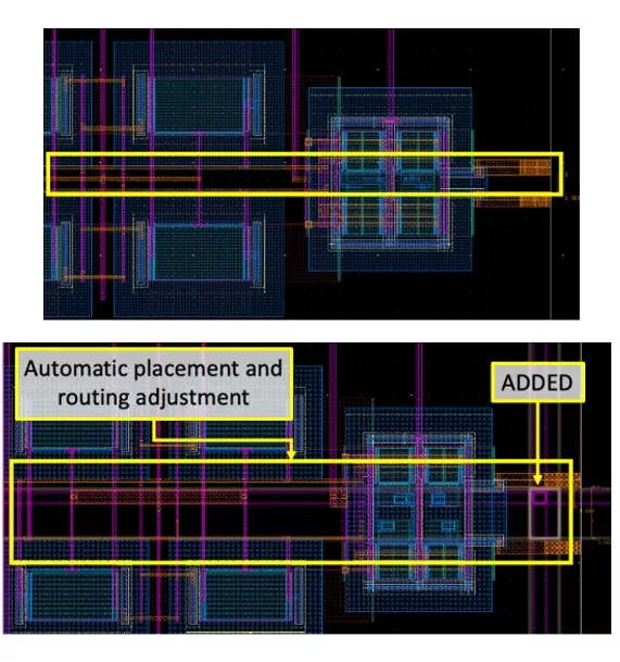
Figure – Illustration of automatic device stretching. Creating space, layers/metal/shapes automatically adjusted
New features in release version 25.1
- Layout Automation Suite enhancements: Automatic device stretching, DRC detection and correction, and metal stacking features streamline layout optimization, ensuring compliance with design rules and enhancing connectivity.
- Inductor characterization improvement: For RF applications like Wi-Fi and Bluetooth devices, the updated inductor characterization feature offers automated analysis based on PDK data, enhancing efficiency and accuracy for designers.
- Enhanced area estimation model: Integrated into the Circuit Porting Suite, the updated model provides precise area estimates, enabling customers to optimize space utilization and improve design performance.
Customer benefits include
- Increased efficiency: Automation reduces manual effort, saving time for critical project aspects.
- Enhanced accuracy: Automatic error detection and correction ensure adherence to design rules, improving product quality.
- Cost savings: Efficient space use minimizes manufacturing costs and post-production revisions.
- Customer satisfaction: Tailored features address specific design challenges, providing a competitive edge in the market.
Related Semiconductor IP
- DSP-Based 112G SerDes
- XTAL oscillator in TSMC-7nm
- GPU
- V-by-One Verification IP
- AI model compression IP
Related News
- Thalia's AMALIA (23.4a) qualified on Siemens AFS for increased analog design migration flexibility
- Siemens delivers AI- accelerated verification for analog, mixed-signal, RF, memory, library IP and 3D IC designs in Solido Simulation Suite
- Thalia Design Automation launches AMALIA Platform 25.2
- Thalia Design Automation announces AMALIA Platform release 25.3 qualified for advanced process nodes down to 4nm
Latest News
- Arteris Deployed by Speedata for Data Center Compute
- Siemens to acquire Defacto Technologies to complement its EDA portfolio with automated SoC design creation
- Mach42 Completes £7M Funding Round, Led by IP Group With Investment From BGF and Foresight Group
- ELECTRA IC Unveils Comprehensive IP Core Suite for Next-Generation Post-Quantum Cryptography
- CAST Enhances Serial Memory Controller IP with Encryption, Low-Power, and ASIL-Ready Options