Imec achieves breakthroughs in ferroelectric memory research for next-generation memory solutions to meet AI-era data needs
As AI workloads drive a steep increase in memory capacity, imec explores ferroelectric memory technologies to address the cost and density constraints of classical DRAM.
LEUVEN (Belgium), June 17, 2026 - This week, at the 2026 IEEE / JSAP symposium on VLSI Technology & Circuits, imec, a world-leading research and innovation hub in advanced semiconductor technologies, presents two advances in ferroelectric memory research, targeting both ferroelectric capacitors and ferroelectric field-effect transistors as emerging candidates to enable low-voltage operation and high-density integration. Ferroelectric memory is drawing increasing attention as AI workloads place unprecedented pressure on memory systems to deliver more capacity, higher bandwidth, and better energy efficiency at sustainable cost. As conventional memory technologies such as DRAM and SRAM become harder to scale, ferroelectric approaches are emerging as promising candidates because they can combine low-voltage operation with pathways to denser 3D integration. Against that backdrop, imec is presenting two complementary advances: low-voltage ferroelectric capacitors that could support future DRAM-like memory, and vertically stacked FeFETs that point toward compact, high-density memory architectures for next-generation AI systems.
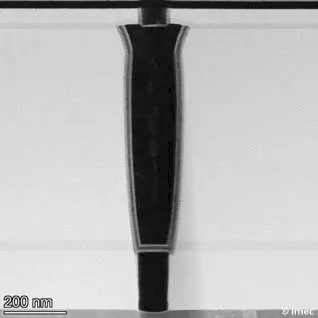
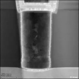
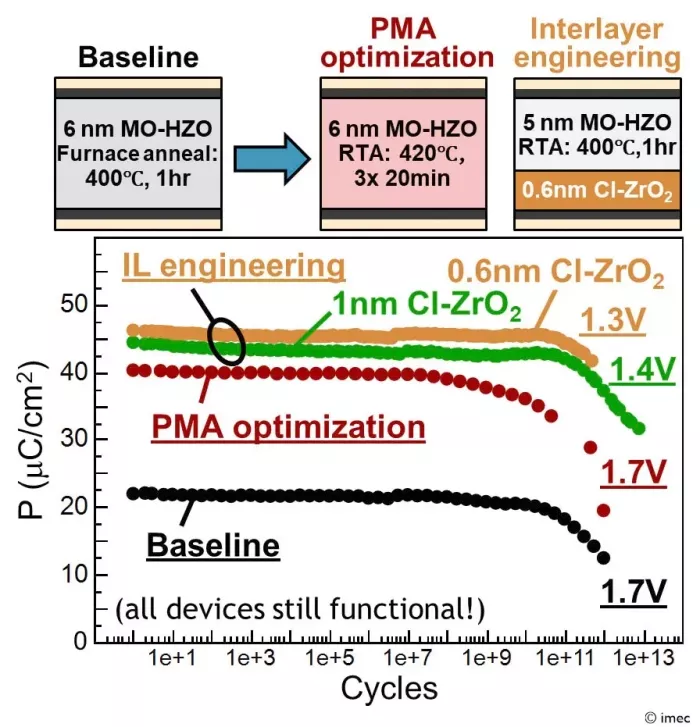
Ferroelectric capacitors are shown to enable low-voltage (~1.3 V) operation through ferroelectric layer scaling while maintaining high remnant polarization (>40 μC/cm²) and endurance (≥10¹³ cycles), key requirements for DRAM-like memory applications. In a separate demonstration, imec takes a step toward high-density 3D ferroelectric memory with vertically stacked IGZO-based ferroelectric field-effect transistors (FeFETs). The work presents the first functional demonstration of a five-word-line vertical stack of FeFET memory cells, increasing storage density by stacking devices on top of each other. By introducing a dual-gate configuration with a back-gate, imec improves erase efficiency, a key challenge for FeFET technology. This innovation in architecture highlights the potential of oxide semiconductor-based FeFETs for future high-density memory applications.
It is imec’s multidisciplinary approach that brings the presented device concepts together through shared materials, integration strategies, and a common vision of enabling scalable 3D ferroelectric memory. Both approaches rely on similar ferroelectric material stacks, where insights gained from interfacial engineering and scaling in capacitors directly apply to the optimization of FeFET devices. At the same time, the advanced 3D integration techniques demonstrated for FeFET stacking provide pathways for implementing high-density 3D ferroelectric capacitor arrays. Both memory building blocks, ferroelectric capacitors and FeFETs, offer distinct advantages, with insights from each guiding further optimization of the other.
These advances come at a critical moment for the semiconductor industry. As memory technologies such as DRAM and SRAM approach their scaling limits, and AI-driven workloads require exponentially larger memory capacity, the need for new memory concepts becomes increasingly necessary. The demonstrated low-voltage operation of ferroelectric capacitors supports energy-efficient memory concepts, while vertically stacked FeFETs open the door to compact, high-density storage suitable for embedded and next-generation computing architectures. Collectively, these innovations offer complementary pathways to address performance and cost challenges in future data-centric systems.
“This work shows how imec’s multidisciplinary expertise, from materials science to advanced 3D integration, enables us to tackle some of the most pressing challenges in memory technology,” said Attilio Belmonte, program director at imec. Maarten Rosmeulen, program director at imec, continues: “We are exploring multiple paths toward the memory solutions that will be required to sustain the rapid growth of AI and data-intensive applications.”
Looking ahead, imec will continue to refine both device concepts while addressing remaining challenges such as endurance and erase performance in FeFETs and further voltage scaling and reliability optimization in ferroelectric capacitors. Future work will focus on system-level evaluation of these technologies, the development of fully integrated 3D memory architectures, and improving key performance metrics to bring these concepts closer to practical implementation. While still at the research stage, these results mark important steps toward next-generation memory technologies that could redefine how data is stored and accessed in the AI era.
About imec
Imec is a world-leading research and innovation hub in advanced semiconductor technologies. Leveraging its state-of-the-art R&D infrastructure and the expertise of over 6,500 employees, imec drives innovation in semiconductor and system scaling, artificial intelligence, silicon photonics, connectivity, and sensing.
Imec’s advanced research powers breakthroughs across a wide range of industries, including computing, health, automotive, industry, consumer electronics, aerospace and security. Through IC-Link, imec delivers customized solutions, from concept to full-scale manufacturing, to meet the most advanced design and production needs. Through imec.ventures, imec creates, co‑creates new ventures, and supports existing semiconductor deep‑tech companies to scale-up.
Imec collaborates with global leaders across the semiconductor value chain, as well as with technology companies, start-ups, academia, and research institutions in Flanders and worldwide. Headquartered in Leuven, Belgium, imec has research facilities in Belgium, across Europe, the USA and the GCC region, and representation on three continents. In 2025, imec reported revenues of €1.2 billion.
For more information, visit www.imec-int.com
Related Semiconductor IP
- LPDDR4/4x/5/5x PHY
- Cryptographic co-processor for lightweight cryptography
- Telematics Processors IP
- Low (Active) Power Memory
- Embedded MTP (Multi-Time Programmable) IP, 512x8 bits for 5V V3E_BCD
Related News
- Imec and Analog Devices sign strategic research partnership for development of next-generation IoT devices
- Neumonda and Ferroelectric Memory Company Collaborate in the Commercialization of Non-Volatile DRAM
- NanoIC adds advanced SRAM memory macros to its N2 pathfinding PDK
- NanoIC extends its PDK portfolio with first A14 logic and eDRAM memory PDK
Latest News
- Imec and Diraq demonstrate first coherent operation of eight silicon MOS spin qubits fabricated in a 300mm CMOS-compatible foundry process
- RISC-V Is Inevitable, State of the Union Keynote Argues
- Intel Invests €5 Billion to Expand Manufacturing in Europe
- SEALSQ and Quobly sign $5 Million commercial agreement to integrate post-quantum security into next-generation silicon quantum computing platforms
- InfiniNode secures EUR 2 million financing to advance on-chip data movement technologies for next-generation compute systems