LPDDR4/4x/5/5x PHY
The DDR PHY is designed to support LPDDR4, LPDDR4x and LPDDR5 SDRAM.
Overview
The DDR PHY is designed to support LPDDR4, LPDDR4x and LPDDR5 SDRAM.
This allows the host SoC to easily be configured for the specific DDR SDRAM variant used in the system via simple software control, allowing one chip to target multiple applications using different DDR types.
The DDR PHY has been optimized to take advantage of the memory configurations and packaging to reduce the total memory subsystem power and area.
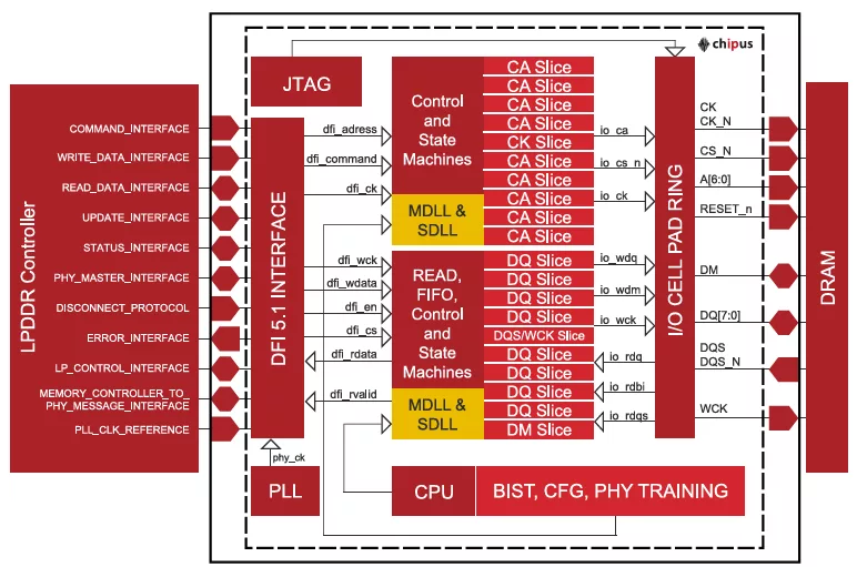
The DDR PHY is designed to comply with DFI 5.1 memory standard so the PHY can work seamlessly with DDR Memory controllers from any supplier that compliant with the DFI 5.1 Standard.
Key features
- Operating range 533 – 8,533 Mbps LPDDR4/LPDDR4x/LPDDR5/LPDDR5x mode
- DFI 1:2 and DFI 1:4 clocking support
- 1:2 DFI_CLK = 1,066 MHz
- LPDDR4/4x/5/5x – 4,266 Mbps
- 1:4 DFI_CLK = 533 MHz
- LPDDR4/4x/5/5x – 4,266 Mbps
- 1:4 DFI_CLK = 800 MHz
- LPDDR5 – 6,400 Mbps
- 1:4 DFI_CLK = 1,066 MHz
- LPDDR5 – 8,533 Mbps
- PHY includes PVT compensated I/Os that are compatible with wire bond and flip chip (ESD included)
- Small PHY area – (tbd)mm2
- Low power – (tbd)/(tbd)/(tbd) mW (READ, WRITE, and IDLE)
- Configurable external memory channel widths in 16-bit, 32-bit and 64-bit
- Programmable I/O output drive strength and On Die Termination (ODT) impedance with dynamic PVT compensation
- Support for Per Bit Deskew
- At speed Internal and External Loopback BIST testing in PHY Standalone mode for Chip Probe Testing on DQ/DQS
- Scan and JTAG/BSR standard testing
- AHB Register interface for easy PHY configuration and control for non-DFI related features
- Low power stand by using DFI Compliant LP interface
- DATA Retention
- PHY Independent DDR Training, Dynamic training and DDR Initialization Support using embedded memory controller and 32-bit processor
- CA Training
- Write Leveling
- Read Gate Training
- Read EYE training EYE Scan and Bit Deskew
- READ EYE DFE
- Write EYE Training EYE Scan and Bit Deskew
- WRITE EYE DFE
- CK and WCK Duty Cycle Training
- READ DQS Duty Cycle Training
- READ and WRITE OSC Training
- READ and WRITE Offset Calibration
- READ and WRITE PreEmphasis Calibration
Block Diagram
What’s Included?
- Databook
- User Guide
- Behavioral RTL model
- LEF file
- .LIB file
- GDSII Layout Database
- CDL
- SCAN and JTAG Vectors
- IBIS Models for PCB Design and verification
Specifications
Identity
Standards & Interfaces
Files
Note: some files may require an NDA depending on provider policy.
Provider
Learn more about LPDDR IP core
LPDDR flash: A memory optimized for automotive systems
A New Generation of LPDDR
Enabling Memory Choice for Modern AI Systems: Tenstorrent and Rambus Deliver Flexible, Power-Efficient Solutions
SOCAMM: Modernizing Data Center Memory with LPDDR6/5X
On-Device AI Semiconductors & High-speed Interconnects in the Physical AI era
Frequently asked questions about LPDDR Interface IP
What is LPDDR4/4x/5/5x PHY?
LPDDR4/4x/5/5x PHY is a LPDDR IP core from Chipus Microelectronics listed on Semi IP Hub.
How should engineers evaluate this LPDDR?
Engineers should review the overview, key features, supported foundries and nodes, maturity, deliverables, and provider information before shortlisting this LPDDR IP.
Can this semiconductor IP be compared with similar products?
Yes. Buyers can compare this product with similar semiconductor IP cores or IP families based on category, provider, process options, and structured technical specifications.