CEA-Leti Scales Ferroelectric RAM to 22nm Node, Unlocking Denser, More Efficient Memory for Edge AI
Breakthrough Reported at VLSI 2026 Also Extends to High-Performance Computing, Aerospace & Defense Systems, and IoT Platforms
HONOLULU, Hawaii — June 15, 2026 — CEA-Leti today announced a major advance in memory technology: the demonstration of ferroelectric RAM (FeRAM) scaled to the 22nm manufacturing node using an innovative 3D capacitor architecture. The breakthrough, presented at the VLSI Conference in Honolulu, removes a longstanding density barrier that has kept FeRAM from competing with volatile memory—and opens the door to faster, more energy-efficient artificial intelligence (AI) at the edge.
 By vertically integrating ferroelectric capacitors made from hafnium zirconium oxide (HZO) thin films, the team achieved memory cells that are 2.5 times smaller than standard SRAM at the same 22nm node, matching the density of SRAM at the much more advanced 10nm node. Moreover, unlike SRAM, FeRAM retains data without power, combining non-volatility with a density previously attainable only by volatile memory.
"This 3D ferroelectric capacitor-based FeRAM technology enables high-speed, high-density, low-voltage operation of non-volatile memory arrays," said Simon Martin, lead author of the paper, "Engineering 3D HZO Ferroelectric Capacitors to Scale Down 22nm Embedded FeRAM." "This breakthrough is a strong candidate for high-performance embedded applications, including ultra-low-power Edge AI, high-performance computing, aerospace and defense systems, and IoT platforms."
Why It Matters
Today's smart devices increasingly rely on sending data to the cloud for AI processing—a costly cycle in both time and energy. FeRAM that is both fast and dense enough to embed directly on a processor enables devices to process data locally. The implications extend beyond user convenience: computing operations account for a significant and growing share of global electricity consumption, much of it still generated from fossil fuels.
"This technology paves the way for highly energy-efficient systems, helping to reduce overall power consumption and, consequently, reliance on fossil-based energy sources," Martin said.
The Breakthrough
Historically, FeRAM fabrication was constrained to flat, planar capacitor structures that limited how small and dense memory cells could be manufactured. In these architectures, the capacitor—not the selection transistor—determines the cell footprint because the current flowing through the capacitor during memory operations is inherently low. To overcome this physical limit, CEA-Leti shifted to a vertical architecture, building the capacitor upwards rather than outwards.
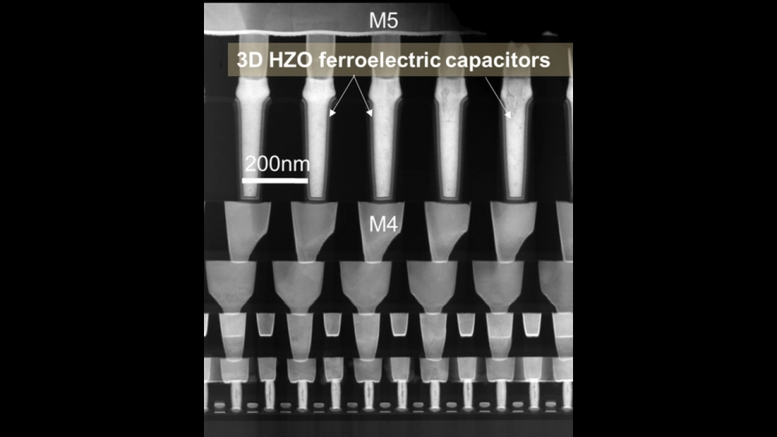
The team demonstrated two back-end-of-line (BEOL) integration schemes for 3D ferroelectric capacitors (FeCaps) at 22nm, utilizing advanced patterning and deposition techniques. Array functionality with Gaussian bit distributions was confirmed down to 0.047 μm² 1T-1C FeRAM bitcells operating at just 1.3V, featuring a standard logic selector and a 3D FeCap with an aspect ratio of roughly 4:1.
The researchers also demonstrated a clear path to even greater density: 3D FeCaps with an aspect ratio of 17:1, a 60nm diameter, and a 120nm pitch—shrinking the capacitor footprint to just 0.0028 μm². A higher aspect ratio maximizes the effective surface area of the ferroelectric capacitor within each bitcell, enlarging the memory window without sacrificing array density.
Solving the "Wake-Up" Problem
Traditional FeRAM devices often exhibit a phenomenon known as "wake-up," where electrical characteristics shift unpredictably during initial cycling, degrading stability and reliability. CEA-Leti's high-aspect-ratio 3D capacitors exhibited wake-up-free behavior consistent with an approximately 80 percent orthorhombic phase fraction in the HZO film, as confirmed by precession electron diffraction (PED).
While the precise mechanism is still under study, the suppression of wake-up is likely related to the confinement of materials within the narrow, high-aspect-ratio vias, which locally modifies the strain state in the ferroelectric thin film. This stabilizes the crystal phase responsible for memory function from the outset.
Next Steps
CEA-Leti plans to integrate the demonstrated high-aspect-ratio ferroelectric capacitors into dense FeRAM arrays on a 22nm FDSOI platform, aiming to achieve the highest-performance embedded FeRAM to date.
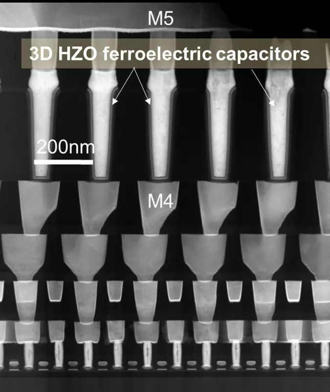
STEM cross-section image of 3D HZO FeCap based FeRAM array integrated at 22nm FDSOI node in BEOL between Metal4 and Metal5, featuring 0.047µm2 1T1C bitcell size with Logic NMOS transistor.
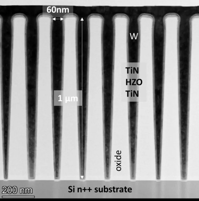
STEM cross-section image of a 17:1 High-Aspect-Ratio 3D FeCap field with 60 nm diameter and 1µm deep FeCaps, filled of TiN/HZO/TiN/W ferroelectric stack
NOTE: Dr. Madjid Hihi, Deputy Director for Clinical Innovation at CEA-Leti’s Innovative Health Technologies Division, will speak at a VLSI luncheon from 12:15–1:15 PM, on June 18. The title of his talk is “Innovative Neurotechnologies – A Journey from the Lab to the Clinic and Back.” Neurotechnology is a booming field, and Madjid will highlight clinical world premieres enabled by CEA-Leti technologies.
This project received funding from the European Union and Chips Joint Undertaking (Fames projects), supported by French public authorities (France 2030, in particular through the NextGen project).
About CEA-Leti (France)
CEA-Leti, a technology research institute at CEA, is a global leader in miniaturization technologies enabling smart, energy-efficient and secure solutions for industry. Founded in 1967, CEA-Leti pioneers micro-& nanotechnologies, tailoring differentiating applicative solutions for global companies, SMEs and startups. CEA-Leti tackles critical challenges in healthcare, energy and digital migration. From sensors to data processing and computing solutions, CEA-Leti’s multidisciplinary teams deliver solid expertise, leveraging world-class pre-industrialization facilities. With a staff of more than 2,000 talents, a portfolio of 3,200 patents, 14,000 sq. meters of cleanroom space and a clear IP policy, the institute is based in Grenoble (France) and has offices in San Francisco (United States), Brussels (Belgium), Tokyo (Japan), Seoul (South Korea) and Taipei (Taiwan). CEA-Leti has launched 80 startups and is a member of the Carnot Institutes network. Follow us on www.leti-cea.com and @CEA_Leti.
Technological expertise
CEA has a key role in transferring scientific knowledge and innovation from research to industry. This high-level technological research is carried out in particular in electronic and integrated systems, from microscale to nanoscale. It has a wide range of industrial applications in the fields of transport, health, safety and telecommunications, contributing to the creation of high-quality and competitive products.
For more information: www.cea.fr/english
Related Semiconductor IP
- Ultra-low jitter, low-power ring-oscillator-based PLL-3GHz-4GHz
- Image Warping IP
- Image Warping IP
- ML-KEM-X Post-Quantum Cryptography Core
- AXI5 to/from AXI4 Bridge
Related News
- CEA-Leti Demonstrates Embedded FeRAM Platform Compatible with 22nm FD-SOI Node
- CEA-Leti and Fraunhofer IPMS Validate Wafer Exchange for Ferroelectric Memory Materials Within the FAMES Pilot Line
- Fujitsu pushes SiP over SoC for fast-cycle RAM
- Virage offers nonvolatile RAM to integrate on an SoC
Latest News
- ASYGN Revolutionizes Ultra-Low-Power Embedded AI with Its ColibryNPU Microcontroller
- Tampere University Joins OpenTitan Coalition to Advance RISC-V SoC Security and Open-Source Silicon Research
- Kandou AI to Open India Chip Design Headquarters in Hyderabad
- CAST Expands Functional Safety IP Line with ASIL B Ready SENT/SAE J2716 Receiver Core
- SkyeChip Advances Custom Interface IP Engagement with Cerebras for Wafer-Scale AI Platforms