Aldec shortens time of ASIC design prototype bring-up in FPGA with HES-DVM Proto mode
Henderson, Nevada, U.S.A. – January 14, 2019 – Aldec, Inc., a pioneer in mixed HDL language simulation and hardware-assisted verification for ASIC and FPGA designs, has unveiled the latest release of HES-DVM™, the company’s fully automated and scalable hybrid verification environment for SoC and ASIC designs. Release 2018.12 features enhancements to the level of automation in Prototyping mode plus the faster compilation of HDL to FPGA.
The new HES-DVM provides design partitioning and partition interconnection tools designed to meet the growing need for, and challenges associated with, FPGA prototyping; i.e. FPGAs used as a pre-silicon SoC verification vehicle to assure ultimate speed or as a hardware software co-verification platform. Thanks to the use of virtual partitions, HES-DVM can also be used in the process of designing new prototyping boards to establish the most efficient board architecture for the project or with third party and in-house developed FPGA boards.
With the 2018.12 release of HES-DVM, users will be able to evaluate quickly various partitioning scenarios and choose the one which provides the best performance on a given prototyping board.
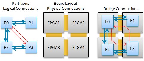
With this release, the productivity of an FPGA prototyping team is greatly boosted thanks to the addition of two new automation enhancements. The first of these is Automatic Routing, which automatically resolves feed-through connections if there are no appropriate chip-to-chip traces on a prototyping board. The second is Automatic Physical Connections for multi-FPGA prototyping boards, which routes all inter-partition connections using available chip-to-chip traces and it intelligently assigns various types of I/O - including integrated serialization (SERDES) and differential signaling (LVDS).
In addition, and to further reduce the design setup turnaround time in HES-DVM’s Emulation and Prototyping modes, Aldec has developed a proprietary HDL compiler, details of which shall be announced later in the year.
“We are proud to announce the latest release of HES-DVM. It boosts our FPGA Prototyping and Emulation solutions, through the addition of features that significantly shorten design setup time, thus enabling designers to evaluate more prototype scenarios than before in a given amount of time,” said Zibi Zalewski, General Manager of Hardware Division. “Also, users can benefit from an ultra-fast turnaround time, from bug–fix to a revised prototype run, and potentially spare themselves from months of tedious work. Indeed, we are devoted to persistently raising the bar in FPGA-based emulation and prototyping technology.”
Availability
The new HES-DVM™ 2018.12 software is available now. To learn more or to evaluate HES-DVM, please visit www.aldec.com, e-mail sales@aldec.com, call +1 (702) 990-4400, or contact one of Aldec’s worldwide distribution partners.
About HES™ Prototyping
Aldec offers a portfolio of HES™ prototyping boards based on the largest Xilinx FPGAs of the Virtex UltraScale and Virtex-7 families. The boards are architected to allow for easy expansion using BPX backplane and standardized FMC and BPX daughter card connectors.
About HES-DVM™
HES-DVM™ is a fully automated and scalable hybrid verification environment for SoC and ASIC designs. Utilizing the latest co-emulation standards like SCE-MI or TLM and the newest FPGA technology, hardware and software design teams obtain early access to the hardware prototype of the design. HES-DVM is used in labs worldwide for all kinds of emulation and physical prototyping tasks including Simulation Acceleration, Hybrid Virtual Prototypes, In-Circuit Emulation, Software Validation and Prototyping.
About Aldec
Aldec Inc., headquartered in Henderson, Nevada, is an industry leader in Electronic Design Verification and offers a patented technology suite including: RTL Design, RTL Simulators, Hardware-Assisted Verification, SoC and ASIC Prototyping, Design Rule Checking, CDC Verification, IP Cores, Requirements Lifecycle Management, DO-254 Functional Verification and Military/Aerospace solutions. www.aldec.com
Related Semiconductor IP
- DSP-Based 112G SerDes
- XTAL oscillator in TSMC-7nm
- GPU
- V-by-One Verification IP
- AI model compression IP
Related News
- Aldec Launches HES-DVM Proto "Cloud Edition" - Giving Engineers Easier Access to FPGA-based ASIC & SoC Prototyping
- Aldec unveils Xilinx UltraScale FPGA-based prototyping board enabling Simulation Acceleration and Emulation with the latest release of HES-DVM
- Aldec's New HES FPGA Accelerator Board Targets HPC, HFT and Prototyping Applications plus Hits the "Price/Performance" Sweet Spot
- Bluetooth Dual Mode v5.2 Protocol Stack SW, Profiles & LC3 codec licensed to leading Tier 1 Company for ultra-low power TWS Hearable Audio SoC
Latest News
- Arteris Deployed by Speedata for Data Center Compute
- Siemens to acquire Defacto Technologies to complement its EDA portfolio with automated SoC design creation
- Mach42 Completes £7M Funding Round, Led by IP Group With Investment From BGF and Foresight Group
- ELECTRA IC Unveils Comprehensive IP Core Suite for Next-Generation Post-Quantum Cryptography
- CAST Enhances Serial Memory Controller IP with Encryption, Low-Power, and ASIL-Ready Options