Estimating the silicon area of specialty I/Os

Why the right specs early save the most area?
Some I/O specs look ordinary and then quietly eat a large part of your area budget. A requirement that seems minor can turn a compact cell into one several times its size and you often don’t see it coming until the floorplan is already taking shape. Predicting that early is the hard part and it is where the real Power/Performance/Area (PPA) savings are.
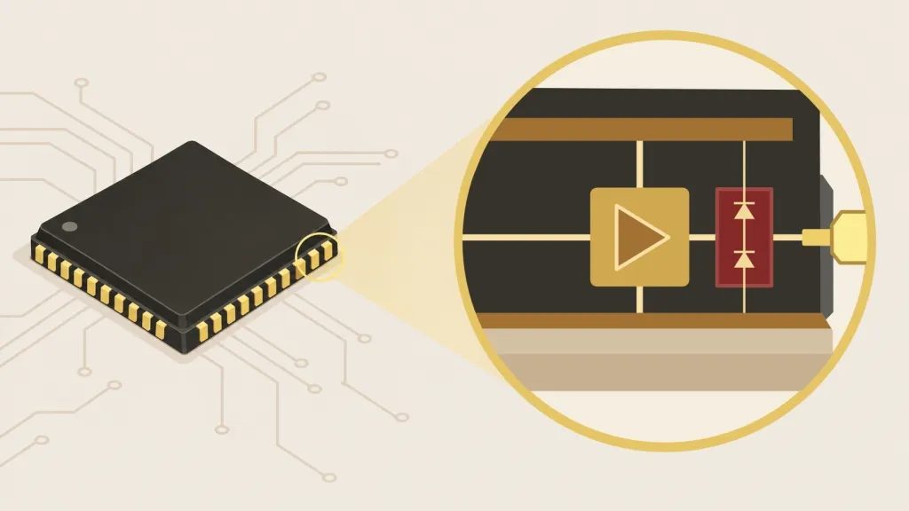
Standard foundry GPIOs are where most designs start and for good reason. When the PDK cells fit your requirements there is no reason to look further. The question is what happens when they don’t. Built for common, general purpose use in the voltage domains the process already supports, their coverage is deliberately broad, which means it stops short of more specialized needs. Many properties are either not addressed at all or handled in a way that is far from PPA efficient.
Some of the aspects a common GPIO tends to leave uncovered are:
- Very high or very low drive strength
- Extreme voltage ranges
- above the maximum allowed voltage, handled by an over-voltage tolerant (OVT) design
- below the typical range, handled by an under-voltage tolerant (UVT) design
- several voltage modes at once, with (automatic) mode-select
- Very low leakage or low power operation
- Fail-safe operation, for example an I2C line that must not load the bus while the device is unpowered
- Enhanced robustness
- ESD protection beyond 2kV HBM or 5A CDM
- Radiation tolerance
- EOS tolerance
- Any combination of the above, but this is where complexity kicks in…
Most of these requirements can be solved on their own. Each one shifts the design trade-offs in a different direction, though satisfying several at once is rarely as simple as adding up the individual solutions. To understand where the area really goes, we need to look at the main contributors inside the I/O and how specifications such as drive strength, voltage range, logic overhead and ESD protection affect them. More importantly we will look at what happens when those requirements start to interact, and why making the right choices early can save far more area than optimizing the design later.
Drive strength demands
Let’s start with the driver. It handles the largest currents in the I/O, so it generally takes up a good part of the area.
Drive strength is usually described as the steady state current the driver can source or sink while holding the bus high or low. In practice though, what sets that number is the job the driver has to do: how much load sits on the bus and how fast it has to switch. A heavier load needs more current to move and a faster edge means that current has to arrive in less time. Both push toward a bigger transistor and in turn a bigger area.
Each switch moves a charge onto the bus and then pulls it back and the faster the I/O runs, the more often that happens. This sets the current the driver has to supply and with it the size of the driver, in general the area can be expressed by:
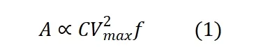
- Vmax is the maximum voltage the transistor stack has to hold. Push that up and you need more space between source and drain, which makes the driver more resistive. The increased resistance and space is where we get the square.
- C is the load. More load means more charge to shift, so you need more current and a bigger driver to supply it.
- f is how fast the bus switches. The quicker it has to go, the more current you need, and again the driver grows.
This equation covers most cases for a driver, since it will most often operate at its maximum voltage rating. For some specialty I/Os that isn’t true. When a driver has to work across multiple voltage modes, the voltage it sees changes with operation and so does the drive strength it can deliver. Two more terms come into play:
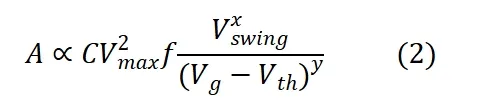
- Vg and Vth set the gate overdrive and the gap between them. More overdrive gives more drive strength, so a low overdrive pushes the driver area up. The exponent y depends on the transistor type and how the driver runs. For advanced FinFET or GAA devices it sits close to one and never goes above two.
- Vswing is the output swing. It matters most when the driver acts like a current source, where a bigger swing needs more drive current to charge the load. A real driver isn’t an ideal current source though, it has some resistance too, so the exponent x usually lands between zero and one.
A counter-intuitive example is under-voltage tolerant (UVT) operation, mentioned in the introduction. You would expect a lower voltage to mean less stress and so a smaller driver. In practice, the opposite can happen. As the operating voltage drops, the gate voltage Vg moves closer to the transistor threshold voltage Vth. That reduces the available gate overdrive, (Vg – Vth) and with it the amount of current a transistor of a given size can deliver.
The driver still has to meet the same load and timing requirement, so the lost current has to be recovered by increasing the transistor size. This is where the area penalty appears. Equation 2 captures this through the term:
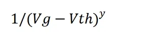
As Vg moves closer to Vth, the required area rises quickly, which is why lower-voltage operation can result in a larger driver rather than a smaller one.
Logic and overhead
Compared to the driver, the logic in an I/O is usually small. Newer technologies keep improving logic packing density, which might raise the expectation that the non-driver area becomes negligible.
Where actually the opposite is true. That packing density is only possible thanks to reduced core voltage swings. Part of the logic in an I/O often operates above the core voltage though, which means it needs level-shifters. These higher voltages force the logic elements to sit further apart, far enough to hold the voltage range safely. On advanced nodes this shows up as voltage dependent design rules. These spacing stems from the physics of the silicon itself, so they don’t shrink as the node does. The result is that this overhead takes up a bigger share of the area the further you advance, compared to the useful area or even the driver area.
So on the most advanced nodes it pays to keep the logic simple. Limiting the number of selectable drive strengths is one easy way to do it.
ESD protection
All chips require ESD protection, but these are very often not MOS based. These devices are commonly diode or SCR-based. This is because these devices combine large current densities with low area, capacitance and leakage.
The physics behind these devices is fundamental, which makes them robust across many technologies. It also means their footprint does not shrink much as feature sizes do. So with each new node the ESD clamp takes up a larger share of the total I/O area.
This area disparity is especially prevalent in FinFET or GAA/nanosheet technology. An example of limitation in FinFET is an interface for die-2-die where the driver/receiver was 10×10µm and the ESD 25×10µm. In this example the ESD is 2.5 times larger than the driver, even after being reduced by over 50%.
How do I choose the right spec?
 Specialty I/O’s lead to new trade-offs, but also allow to shift the trade-offs compared to regular GPIO properties. In order to achieve the most performant product, it is important to understand the impact of the specifications on PPA.
Three important considerations are highlighted below, one of which we have already mentioned as an unlikely culprit.
UVTs exponential cost
Or at least an inflated cost. The driver area is proportional to 1/(Vg-Vth), so whenever the available voltage gets close to the threshold voltage this can have a huge area cost which is often underestimated.
The area cost of UVT-operation needs might even increase if they are part of a mode-select requirement. In that case, it is important to consider whether all specs need to be met under UVT conditions. If you can drop or reduce this it can have a huge impact on the area.
When worst cases stack up
Specification lists are often just a stack of worst cases, each one taken on its own with no thought to how they interact. Ask for every worst case at once and the area can balloon, even though no single number looked alarming at first glance. The reverse is also true. Relaxing a spec under conditions where you don’t really need it can win back a lot of PPA. Here are two examples of this interaction of choosing specifications:
- An I/O that needs 50MHz into a 100pF load, but 100MHz into 50pF, ends up half the size of one asked to drive the full 100pF at 100MHz. Same peak numbers, very different silicon.
- An I/O with multiple voltage modes is usually slower at low voltage anyway, often paired with the slow corner and temperature. If the spec allows less speed or drive strength in that mode, the PPA improves. It might have to hit full speed at 1.8V but be allowed to signal slower in 1.2V mode.
Case study of 1.8V domain across nodes
The 1.8V case makes the scaling problem visible shown in figure 1. As the process moves to smaller nodes, a nominal-voltage driver benefits strongly from transistor scaling. While the 1.8V driver shrinks much less because it still has to tolerate and operate at the same external voltage. The overhead circuitry follows the same pattern and the fail-safe ESD protection changes very little at all. At the most advanced nodes, these parts therefore set an increasingly large part of the I/O footprint, even though the core technology itself has become much denser. This is the same effect discussed earlier for voltage-dependent overhead and ESD, where specialty requirements do not necessarily scale with the node. It also reinforces why the specification matters so much. On advanced nodes, requirements such as a 1.8V domain or fail-safe operation can offset much of the expected area benefit from scaling.
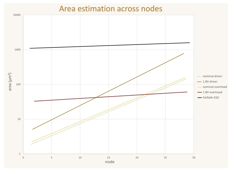
Figure 1. Estimated area scaling across process nodes for nominal-voltage drivers, 1.8 V drivers, associated overhead circuitry and fail-safe ESD protection. The logarithmic area axis highlights the comparatively large and weakly node-dependent footprint of the fail-safe ESD structure.
Conclusion
Specialty I/Os go beyond what a typical GPIO can do and those extra properties come at a cost in PPA, as well as the silicon footprint most of all. The trouble is rarely a single spec, it’s the combination. OVT and UVT are the clear case. Each is manageable alone, but ask for both without accounting for how their trade-offs interact and the area can grow fast. This is why estimating the footprint early, before the spec list hardens is worth the effort. It’s also where the largest area reductions are.
With each new node this only matters more. The I/O logic overhead and the ESD clamp both take up a growing share of the total area, so getting the specs and ESD estimation right up front pays off more on advanced technologies not less.
Sofics builds specialty I/Os that pair beyond-GPIO features with optimized PPA. They are protected by a comprehensive ESD portfolio, further improved through co-design and customer designed specialty I/Os benefit increasingly from standalone ESD protection elements.
Explore Sofics IP:
Related Semiconductor IP
- TSMC 2nm 1V2 GPIO
- Samsung Foundry 4nm 1V8 GPIO I3C
- TSMC 3nm 3V3 GPIO
- TSMC 2nm 1V8 GPIO
- GPIO Verification IP
Related Blogs
- Silicon as strategy: the hidden battleground of the new space race
- Automotive silicon in the era of AI, functional safety, and cybersecurity
- Building Trusted AI Agents from the Silicon Root of Trust
- Arm Compute Platform at the Heart of Malaysia’s Silicon Vision