TSMC 6-inch Wafer Fab Exit Affirms Strategy Shift
TSMC is shedding legacy fabs and moving to larger wafers.
By Majeed Ahmad, EETimes | August 13, 2025
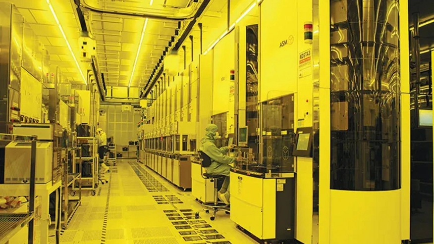
After shaking the gallium nitride (GaN) power electronics world by announcing its intention to quit wafer fabrication, TSMC has thrown another stunner—Taiwan’s mega-fab plans to phase out its 6-inch wafer manufacturing over the next two years. This came to light after the company issued a statement of clarification to a news outlet in relation to its plans on the facility.
Following this decision, TSMC has already notified customers that its Fab 2, which produces 6-inch wafers, will cease production in 2027. The company will later provide final wafer schedules and plans to assist them with transfers to other fabs. Currently, TSMC has one 6-inch wafer fab, four 8-inch wafer fabs, and four 12-inch fabs in Taiwan.
To read the full article, click here
Related Semiconductor IP
- MIPI D-PHY and FPD-Link (LVDS) Combinational Transmitter for TSMC 22nm ULP
- 12-bit, 400 MSPS SAR ADC - TSMC 12nm FFC
- General use, integer-N 4GHz Hybrid Phase Locked Loop on TSMC 28HPC
- Process/Voltage/Temperature Sensor with Self-calibration (Supply voltage 1.2V) - TSMC 3nm N3P
- 25MHz to 4.0GHz Fractional-N RC PLL Synthesizer on TSMC 3nm N3P
Related News
- Apple's Shift in Chip Manufacturing Strategy Boosts Semiconductor Foundry Business in 2013
- Taiwan Maintains Largest Share of Global IC Wafer Fab Capacity
- Taiwan Maintains The Largest Share of Global IC Wafer Fab Capacity
- GlobalFoundries Abandons Chengdu Wafer Fab
Latest News
- EU DARE Project Is Scrambling to Replace Codasip
- Sofics and Alcyon Photonics Partner to Support Next-Generation Photonic Systems
- QuickLogic Appoints Quantum Leap Solutions as Authorized Sales Representative
- Cadence and NVIDIA Expand Partnership to Reinvent Engineering for the Age of AI and Accelerated Computing
- Cadence and Google Collaborate to Scale AI-Driven Chip Design with ChipStack AI Super Agent on Google Cloud