IC Companies Close 49 Wafer Fabs from 2009-2011
Japan and North America with most closures, 150mm afer fabs account for 43% of closures
February 16, 2012 -- Data recently compiled and released in IC Insights' Global Wafer Capacity 2011-2012 report, shows that 49 semiconductor wafer fabs were closed between 2009-2011. Since mid-2007, the IC industry has been paring down its older capacity (i.e., ≤200mm wafers). The decline in ≤200mm capacity picked up speed in 2009 and continued through 2010 and 2011 as suppliers closed or upgraded fabs that were manufacturing using smaller wafers in order to produce devices more cost-effectively on larger wafers. It is worth noting that a few of the fabs are being refurbished for production on larger wafers or for production of "non-IC" products. In the coming years, more companies are expected to shutter older fabs as they transition to the fab-lite business model or become completely fabless. As seen in Figure 1, most of the fab closures from 2009-2011 were 150mm wafer fabs (43%). The distribution of those 49 according to wafer size are: 21 for 150mm, 13 for 200mm, 7 for 125mm, 5 for 300mm, and 3 for 100mm. With Qimonda going out of business in early 2009, its 300mm wafer fabs became the first of their kind to cease commercial operations.
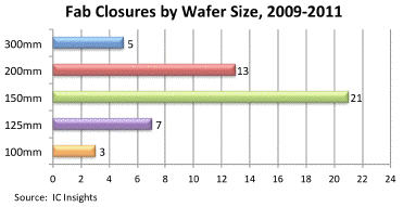
Figure 1
Regionally, according to the Global Wafer Capacity 2011-2012 report, Japan and North America each had 17 wafer fab closures, followed by Europe with 12 and South Korea with 3 (Figure 2). One of the wafer fab closures in Japan was a 300mm IC fab operated by Sony. However, this fab is being retrofitted and will return to service to produce image sensors for the company. The Qimonda wafer fab in Sandston, Virginia, was the only 300mm wafer fab closed in North American (2009) during this time. At the other end of the spectrum, a total of three 100mm wafer fabs were closed in the three-year span. These included fabs owned by DALSA in Bromont, Ontario, Canada, ON Semiconductor in Piestany, Slovak Republic, and Diodes in Oldham, England.
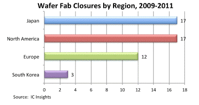
Figure 2
Report Source
Global Wafer Capacity 2011-12
More Information Contact
Trevor Yancey, vice president of IC Insights, phone: +1-480-348-1133, e-mail: trevor@icinsights.com
Related Semiconductor IP
- UCIe D2D Adapter & PHY Integrated IP
- Low Dropout (LDO) Regulator
- 16-Bit xSPI PSRAM PHY
- MIPI CSI-2 CSE2 Security Module
- ASIL B Compliant MIPI CSI-2 CSE2 Security Module
Related News
- Taiwan Maintains Largest Share of Global IC Wafer Fab Capacity
- Record Spending for Fab Equipment Expected in 2017 and 2018
- Record Fab Spending for 2017 and 2018
- 200mm Fabs Thriving; SEMI's Updated 200mm Fab Report Now Available
Latest News
- Arasan Announces immediate availability of its UFS 5.0 Host controller IP
- Bolt Graphics Completes Tape-Out of Test Chip for Its High-Performance Zeus GPU, A Major Milestone in Reducing Computing Costs By 17x
- NEO Semiconductor Demonstrates 3D X-DRAM Proof-of-Concept, Secures Strategic Investment to Advance AI Memory
- M31 Collaborates with TSMC to Achieve Tapeout of eUSB2V2 on N2P Process, Advancing Design IP Ecosystem
- Menta’s eFPGA Technology Adopted by AIST for Cryptography and Hardware Security Programs