Vendor: Global UniChip Corp. (GUC) Category: HBM

TSMC CLN3FFP HBM4 PHY

IGAHBMZ03A is a High Bandwidth Memory 4 Physical Layer (HBM4 PHY) that is compliant with JEDEC HBM4 DRAM Specification JESD270-4.

Controller + PHY + 1 TSMC 3nm N3FFP Silicon Proven View all specifications

Overview

IGAHBMZ03A is a High Bandwidth Memory 4 Physical  Layer (HBM4 PHY) that is compliant with JEDEC HBM4 DRAM Specification JESD270-4. Fabricated in the TSMC 3 nm Advanced process node (N3P), it supports the data rate up to 12 Gbps per data pin in the DDR PHY Interface (DFI)-like 1:4 clock frequency ratio (HBM4 controller clock: WDQS = 1:4). The signal and power integrity is analyzed by the GUC design flow to meet all signal and power requirements.

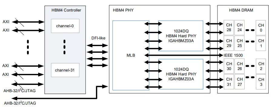
GUC HBM4 PHY includes a hard PHY and a Register Transfer Level (RTL) soft module. The hard PHY, IGAHBMZ03A, includes Command Address (CA) modules, data modules, IO pads, a Phase-Locked Loop (PLL), and Delay-Locked Loops (DLLs). The RTL soft module, also called Miscellaneous Logic Block (MLB), included to work with the hard PHY for functions, such as the training logic, the register controller interface, the Built-In Self-Test (BIST) logic, and the IEEE 1500 function logic.

Key features

  • HBM4 data rate: up to 12 Gbps
  • DFI-like 1:4 clock frequency ratio  (HBM4 controller clock: WDQS = 1:4)
  • Only Burst Length 8
  • AWORD/DWORD bus parity
  • Programmable parity latency
  • HBM4 Data Bus Inversion (DBI)
  • 64DQ ECC/SEV per channel
  • HBM4 Hard PHY delivered as a hard macro including IO, PLL, and DLL
  • Internal Loopback and WRITE/READ BIST
  • HBM4 loopback test, including MISR and LFSR modes
  • IEEE 1500 Instruction
  • HBM4 lane repairs with redundant pins for row/column/data
  • HBM4 Duty Cycle Adjuster (DCA) and Duty Cycle Monitor (DCM) training.
  • HBM4 AWORD write eye/VREF/perbit training training
  • HBM4 WDQSK2CK training
  • HBM4 DWORD write/read eye/VREF/perbit training
  • Broken lane detect and repair
  • DLL compensation to overcome VT  variation
  • HBM4 DWORD write eye retrain to  overcome Device VT variation

Technology

  • Process: TSMC 3 nm 0.75 V/1.2 V CMOS LOGIC FinFET Advanced Process 
  • Special layer & device:  SVT, LVT, LVTLL, ULVT, ULVTLL and ELVT
  • Metal scheme: 1P17M  (1Xa_h_1Xb_v_1Xc_h_1Xd_v_1Ya_h_1Yb_v_4Y_hvhv_4Yy2Z)

Block Diagram

Applications

  • For applications with high performance & high bandwidth memory, such as AI/ HPC.

Silicon Options

Foundry Node Process Maturity
TSMC 3nm N3FFP Silicon Proven

Specifications

Identity

Part Number
IGAHBMZ03A
Vendor
Global UniChip Corp. (GUC)
Controller / PHY
Controller + PHY , PHY
Type
Silicon IP

Files

Note: some files may require an NDA depending on provider policy.

Provider

Learn more about HBM IP core

Reducing Avoidable Memory Trips In HBM Systems

As AI and high-performance SoCs increasingly rely on HBM, memory bandwidth alone is no longer enough to maximize performance. This article discusses why the intelligent data movement and cache efficiency are critical to unlocking the full benefits of HBM-based architectures.

Making Strong Error-Correcting Codes Work Effectively for HBM in AI Inference

LLM inference is increasingly memory-bound, and HBM cost per GB now dominates system cost. Today’s HBM stacks include short on-die ECC, which tightens binning, raises price, and locks reliability policy inside the device. This paper asks a simple question: can we tolerate a much higher raw HBM bit error rate (BER) and still keep end-to-end correctness and throughput, without changing the HBM PHY or the fixed 32B transaction size?

High Bandwidth Memory Evolution from First Generation HBM to the Latest HBM4

HBM4 is the latest generation of the High Bandwidth Memory (HBM) that has become analogous to the Artificial Intelligence (AI) boom that is everywhere in today’s world. HBM is also increasingly being used in other applications like Data centers, autonomous driving systems, servers, cloud computing just to mention few domains where bandwidth and performance in a key requirement.

Breaking the HBM Bit Cost Barrier: Domain-Specific ECC for AI Inference Infrastructure

High-Bandwidth Memory (HBM) delivers exceptional bandwidth and energy efficiency for AI workloads, but its high cost per bit, driven in part by stringent on-die reliability requirements, poses a growing barrier to scalable deployment. This work explores a systemlevel approach to cost reduction by eliminating on-die ECC and shifting all fault management to the memory controller.

Frequently asked questions about HBM Interface IP

What is TSMC CLN3FFP HBM4 PHY?

TSMC CLN3FFP HBM4 PHY is a HBM IP core from Global UniChip Corp. (GUC) listed on Semi IP Hub. It is listed with support for tsmc Silicon Proven.

How should engineers evaluate this HBM?

Engineers should review the overview, key features, supported foundries and nodes, maturity, deliverables, and provider information before shortlisting this HBM IP.

Can this semiconductor IP be compared with similar products?

Yes. Buyers can compare this product with similar semiconductor IP cores or IP families based on category, provider, process options, and structured technical specifications.

×
Semiconductor IP