Overview
PCI Express is a high performance, fully scalable, well defined standard for a wide variety of computing and communications platforms. It has been defined to provide software compatibility with existing PCI drivers and operating systems. Being a packet based serial technology, PCI Express greatly reduces the number of required pins and simplifies board routing and manufacturing. PCI Express is a point-to-point technology, as opposed to the multidrop bus in PCI. Each PCI Express device has the advantage of full duplex communication with its neighbor to greatly increase overall system bandwidth. The basic data rate for a single lane is double that of the 32 bit/33 MHz PCI bus. A four lane link has eight times the data rate in each direction of a conventional bus.
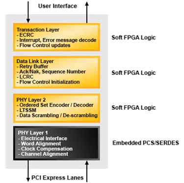
Lattice’s PCI Express Root Complex (RC) Lite core provides an x1 or x4 root complex solution from the electrical SERDES interface, physical layer, data link layer and a minimum transaction layer in PCI express protocol stack. This IP is a lighter version of the root complex intended to use in simple bridging application to local bus. This solution supports the high value, low power LatticeECP3 and LatticeECP2M FPGA device families.
Solutions
* Download demo bitstream from the PCI Express Demo page.
* Visit the PCI Express Solutions page for other demos, boards and development kits.
Learn more about PCI Express IP core
Extending Lattice's post-quantum cryptography leadership from silicon to a complete platform security stack, Lattice Sentry now delivers CNSA 2.0-aligned, NIST-compliant protection across AI data centers, and critical infrastructure, giving system designers a validated, production-ready path to quantum-resistant security.
Combining Arm® AGI CPU server platforms with Lattice FPGAs and AMI firmware creates a solution that provides advanced security, manageability, connectivity, and flexibility for next-generation AI data center infrastructure.
Lattice Prompt pairs with AI agentic tools developers already use, combining them with Lattice design tools, knowledge base, and documentation to turn natural language inputs into validated responses, dramatically accelerating FPGA development while optimizing design performance and capability.
First announced on May 4, 2026, the acquisition creates the industry's most complete secure management and control platform.
The acquisition brings together Lattice’s industry-leading low power FPGAs with AMI’s industry‑leading platform firmware and infrastructure manageability solutions for cloud and AI to create a complete portfolio of secure management and control solutions.
The collaboration demonstrates a real-time AI sensor fusion architecture that integrates TI mmWave radar and camera sensors using NVIDIA Holoscan Sensor Bridge running on Lattice’s low power FPGA. The FPGA acts as a companion chip delivering synchronized sensor data directly into GPU-accessible memory to enable low-latency and robust perception for robotics and industrial edge AI applications.