CDM Dependence on Device Capacitance
This blog will focus on what happens during the CDM pulse itself, and will show how the pulse properties change as a function of DUT to Field Plate capacitance.
1V/3.3V GPIO with I2C ODIO and 3.3V & 5V Analog Cells in TSMC 65nm Key attributes of this IO library include dual independent IO …
1V/3.3V GPIO with I2C ODIO and 3.3V & 5V Analog Cells in TSMC 65nm
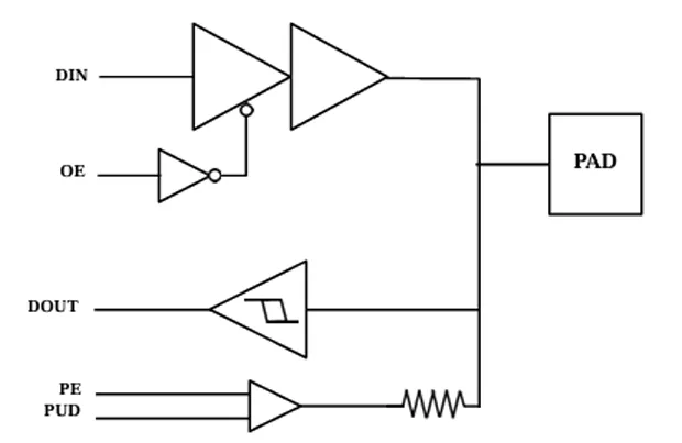
Key attributes of this IO library include dual independent IO supply rails (1.0V-3.3V 3.3V) and power-on-control (POC) to place IOs in HiZ during power-down. The GPIO cell can be configured as input, output or open-drain with a Schmitt trigger input and optional internal 55K ohm pull-up or pull-down resistor. Cells for two independent IO supplies, core power, ground and isolated ground with built-in ESD are included. Aspecialty output cell with matched throughput timings for pulse-width modulation (PWM) applications, along with 5V OTP programming, I2C SVID open-drain and 3.3V 5V analog cells (and associated ESD) complement the GPIO offering. The library is enriched with filler, corner and domain-break cells in digital and analog domains to allow for flexible pad ring construction. ESD design levels are 2KV HBM and 500V CDM.
Operating Conditions
| Parameter | Value |
| VDDIO | 1-3.3V / 3.3V (Dual Rail) |
| Core | 1.2V |
| BEOL | 1P7M |
| WB Pitch | 55um inline |
| Temperate | -40C to 125C |
| ESD | +/- 2kV HBM, +/- 500V CDM |
Cell Names
| Cell Size | Type |
| 55x100um | Digital |
| 55x76um | Analog |
| Foundry | Node | Process | Maturity |
|---|---|---|---|
| TSMC | 65nm | GP | — |
Note: some files may require an NDA depending on provider policy.

Multi-Voltage GPIO 5V ODIO and Analog/RF I/Os in TSMC 65nm is a Analog IP core from Certus Semiconductor listed on Semi IP Hub. It is listed with support for tsmc.
Engineers should review the overview, key features, supported foundries and nodes, maturity, deliverables, and provider information before shortlisting this Analog IP.
Yes. Buyers can compare this product with similar semiconductor IP cores or IP families based on category, provider, process options, and structured technical specifications.