Vendor: Digital Blocks, Inc. Category: I2C / I3C

I2C Controller IP- Master / Slave, Parameterized FIFO, Avalon Bus

The DB-I2C-MS-AVLN Controller IP Core interfaces a microprocessor via the Avalon Bus to an I2C Bus in Standard-Mode (100 Kbit/s) …

Overview

The DB-I2C-MS-AVLN Controller IP Core interfaces a microprocessor via the Avalon Bus to an I2C Bus in Standard-Mode (100 Kbit/s) / Fast-Mode (400 Kbit/s) / Fast-Mode Plus (1 Mbit/s) / Hs-Mode (3.4+ Mb/s) / Ultra Fast-Mode (5 mbit/s).

The I2C is a two-wire bidirectional interface standard (SCL is Clock, SDA is Data) for transfer of bytes of information between two or more compliant I2C devices, typically with a microprocessor behind the master controller and one or more slave devices.

The DB-I2C-MS-AVLN is a Master / Slave I2C Controller that in Master Mode controls the Transmit or Receive of data to or from slave I2C devices while in Slave Mode allows an external I2C Master device to control the Transmit or Receive of data.

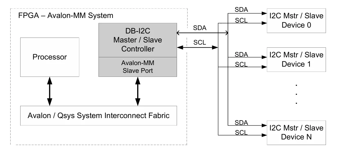
In an Altera FPGA, typically, the microprocessor is a NIOS II or ARM processor, but can be any FPGA embedded processor. The image below depicts the system view of the DB-I2C-MS AVLN Controller IP Core embedded within an FPGA integrated circuit device with its Microprocessor Configuration.

The DB-I2C-MS-AVLN Controller IP Core targets embedded processor applications with higher performance algorithm requirements or I2C transfer requirements to a set of Registers or Memory. While most I2C controllers require high processor interaction involvement, the DB-I2C-MS-AVLN contains a parameterized FIFO and Finite State Machine Control for the processor to off-load the I2C transfer to the DB-I2C-MS-AVLN Controller. Thus, while the DB-I2C-MS-AVLN in Master Mode is busy, independently controlling the I2C Transmit or Receive transaction of data, or in Slave Mode, allowing the external I2C Master device to control the Transmit or Receive of data, the processor can complete other tasks. All Master & Slave Mode Transmit / Receive transfers are with respect to the internal FIFO, thus fully isolating the processor from the I2C transfer of a block of data.

Key features

  • Master / Slave I2C Controller Modes:
    • Master – Transmitter
    • Master – Receiver
    • Slave – Transmitter
    • Slave – Receiver
  • Supports four I2C bus speeds:
    • Hs-Mode (3.4+ Mb/s)
    • Ultra Fast-Mode (5 Mbit/s)
    • Fast Mode Plus (1 Mbit/s)
    • Fast Mode (400 Kb/s)
    • Standard Mode (100 Kb/s)
  • I2C compliant features:
    • Clock Synchronization, Arbitration, SCL held low by Slave, Repeated Start, 7/10-bit addressing, & General Call
  • Parameterized FIFO memory for off-loading the I2C transfers from the processor:
    • Targets embedded processors with higher performance algorithm requirements, by the I2C Controller independently controlling theTransmit or Receive of bytes of information buffered to and from a FIFO.
  • System-level features & integration capabilities:
    • CPU Interface via parameterized FIFO with support for APB / AHB / AXI / AXI-lite / Avalon SoC Interconnect fabrics
    • Enhanced SCL / SDA spike filtering capabilities
    • Enhanced Repeated Start capabilities
  • Optional system-level features & integration capabilities:
    • DMA transfer between the I2C Bus & Memory (SDRAM / SRAM / FLASH)
    • Direct interface to user Registers within ASIC / ASSP / FPGA device, for Master/Slave transfer across the I2C Bus
    • Remote Configuration of a Digital Blocks’ I2C Slave by an I2C Master
    • SMBus Support:  SMBCLK Clock Low Timeout SMBDAT minimum data hold time
  • 13 sources of internal interrupts with masking control
  • Compliance with Altera Avalon and I2C specifications:
    • Compliance with Avalon Memory Mapped Interface Specification (MNL-AVABUSREF-2.0 Version 11.0 Dec 10, 2015)
    • Philips/NXP – The I2C-Bus Specification, Version 2.1, January 2000 and UM10204 Rev 7 – 1 Oct 2021
  • Fully-synchronous, synthesizable Verilog or VHDL RTL core, with rising-edge clocking, no gated clocks, and no internal tri-states, for easy integration intoFPGA or ASIC design flows.

Block Diagram

What’s Included?

  • The DB-I2C-MS-AVLN is available in synthesizable RTL Verilog or a technology specific netlist for FPGAs, along with Synopsys Design Constraints, a simulation test bench with expected results, datasheet, and user manual.
  • The DB-I2C-MS-AVLN comes along with example C code software for controlling Transmit and Receive Transactions in the Eclipse-based Nios® II Integrated Development Environment (IDE).
  • The DB-I2C-MS-AVLN comes along with Altera Qsys / SOPC Builder components, for easy interface to the Avalon Bus, and thus the NIOS II processor.

Specifications

Identity

Part Number
DB-I2C-MS-AVLN
Vendor
Digital Blocks, Inc.
Type
Silicon IP

Files

Note: some files may require an NDA depending on provider policy.

Provider

Learn more about I2C / I3C IP core

From I2C to I3C: Evolution of Two-Wire Communication in Embedded Systems

The I2C (Inter-Integrated Circuit) Bus invented in 1980 by Philips Semiconductors (NXP Semiconductors today) was a massive step forward in simplifying communications in embedded systems. It is a simple two-wire interface for synchronous, multi-master/multi-slave, single ended serial communication. Fast forward 45 years to today and it is still widely used for attaching low speed peripheral Integrated Circuits (ICs), processors and microcontrollers. But silicon today has changed...

Maximizing the Usability of Your Chip Development: Design with Flexibility for the Future

Early in my career selling chips for Motorola Semiconductor, the ability to spin derivative microcontroller chips for a customer’s specific requirement was relatively straightforward. If the volume looked reasonable, we would tape-out a new chip with a few added features because mask costs and wafers were relatively inexpensive at the larger process nodes. The customer won by getting an MCU tailored to their specific need, and Motorola won by gaining a more committed customer plus another SKU that could be sold to other customers – boosting ROI. With the migration to higher cost FinFET nodes, those times are long gone as the economics no longer work.

MIPI CCI over I3C: Faster Camera Control for SoC Architects

Imagine a camera subsystem that responds in microseconds, consumes less power, and offers a more straightforward route to time-to-market. For SoC architects and IP integration teams, that vision is increasingly possible with MIPI Camera Control Interface (CCI) over I3C.

Frequently asked questions about I2C / I3C IP cores

What is I2C Controller IP- Master / Slave, Parameterized FIFO, Avalon Bus?

I2C Controller IP- Master / Slave, Parameterized FIFO, Avalon Bus is a I2C / I3C IP core from Digital Blocks, Inc. listed on Semi IP Hub.

How should engineers evaluate this I2C / I3C?

Engineers should review the overview, key features, supported foundries and nodes, maturity, deliverables, and provider information before shortlisting this I2C / I3C IP.

Can this semiconductor IP be compared with similar products?

Yes. Buyers can compare this product with similar semiconductor IP cores or IP families based on category, provider, process options, and structured technical specifications.

×
Semiconductor IP