Overview
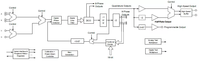
Granite Semicom has just shipped GDS-II of its totally-integrated (no off-chip components) Clock-Driver and Clock-Multiplying-Unit IP block including fractional-N in TSMC’s 40LP process; silicon is expected Q2 2013. In addition to porting its TSMC 40G version, a number of minor changes were incorporated. The oscillator was improved to have higher speed and less jitter, for a given power. Some critical current sources were modified to give an expected 40% reduction in long-term accumulated jitter. In addition, some feedback dividers where changed to give lower power. This block is intended for applications such as the CMU in a SERDES PHY, and for clock-driver applications. This IP block is a digital phased-lock-loop, plus an integrated voltage and current reference, a variety of input amplifiers (single-ended and differential, dc and ac-coupled), a number of programmable dividers, a serial interface for programming, and a high-speed 50 ohm driver capable of driving off-chip at full-speed. The specification is for the Digital PLL (DPLL_40LP) to operate between 0.5GHz and 7.5GHz over process corners between -40 and +125 degrees celsius; the power dissipation is less than 30 mw (for a 5GHz output), and the IP requires a 0.11 mm^2 area (not including pads and the output driver). Long term accumulated jitter is specified at less than 1ps rms accumulated over 260 periods.
Learn more about PLL IP core
How do you ensure that every part of a system receives the clock it needs—without wasting power or sacrificing performance? The answer lies in creating a well-structured frequency plan built around a PLL.
Jian Yang, Sween Kang (Synopsys)
This white paper is aimed at system architects and physical implementation leaders working on the design of SoCs. It can be confusing to understand the impact of different jitter sources and how to calculate a jitter budget when specifying a digital system. This white paper explains how jitter changes the period of a clock and how to ensure that jitter has correctly been accounted for in the calculations for timing closure.
This article explains a some of the key terminology and parameters commonly used to describe jitter. It will also help clarify the most important parameters for a some PLL applications, allowing the designer to better understand what is required from a PLL.
In high end RF systems, such as 5G radios, the requirements are so stringent that the source of this strongest unwanted tone can be the PLL. This article outlines how spurs in the input clock to the ADC or DAC may limit the SFDR. This in turn will set the requirements for the spurs for the input clock (from a PLL), in order to achieve a specific SFDR.
This article compares analog, first-generation digital, and second-generation digital PLLs. It evaluates which type of PLL may be best in which situation. It further discloses a roadmap into other application areas, including general purpose / logic clocking, and regular low-jitter PLLs.