Vendor: OPENEDGES Technology, Inc. Category: HBM

HBM3 PHY IP at 7/6nm

Features a mixed-signal architecture that addresses the challenges of DRAM integration in high-performance and low-power environm…

Controller + PHY + 1 View all specifications

Overview

Features a state-of-the-art mixed-signal architecture that addresses the challenges of DRAM integration in high-performance and low-power environments. This architecture enables OPHYs to overcome issues with long-term impedance drift and clock phase drift, enabling impedance and clock phase updates without interrupting data traffic. Programmable timing at the OPHY boundary combines flexibility with analog precision, resulting in low read/write latency between the ORBIT Memory Controller (OMC) and the DRAM.

OPHYs are designed with subsystem and system-level considerations in mind. Built-in power management logic and advanced PLL design allow aggressive power state management and optimal system power usage. Tight integration with the ORBIT Memory Subsystem enables ActiveQoS bandwidth and latency control for maximum performance of the SoC memory subsystem. At the system level, OPHYs have been designed to minimize package substrate layer and PCB layer requirements, enabling usage in cost-sensitive applications.

Key features

  • Compliant with PHY standards
    • JEDEC compliant LPDDR5X/5/4X/4, DDR5, GDDR6, HBM3 support
    • DFI Interface Compliant
  • ​Flexible Configuration
    • LPDDR54: 8-/16-/32-bit data width per channel
    • GDDR6: 16-bit data width per channel; pseudo-channel mode
    • Supports multiple DFICLK: CK: WCK ratio
    • Multiple DFICLK: CK: WCK ratios
    • Up to 4 ranks with Tx and Rx channel equalization
  • ​Maximum Data Rates
    • Up to 8533 Mbps data rate for LPDDR5x
    • Up to 16 Gbps data rate for GDDR6
  • ​Programmable State Machine (PSM)
    • Proprietary microcontroller and custom ISA enable customizable DFT features and multiple LPDDR standard support efficiently while reducing the area
  • ​Multiple FSPs and the LP States
    • Supports up to 4 frequency set points (FSPs)
    • Supports multiple low power states for system power optimization

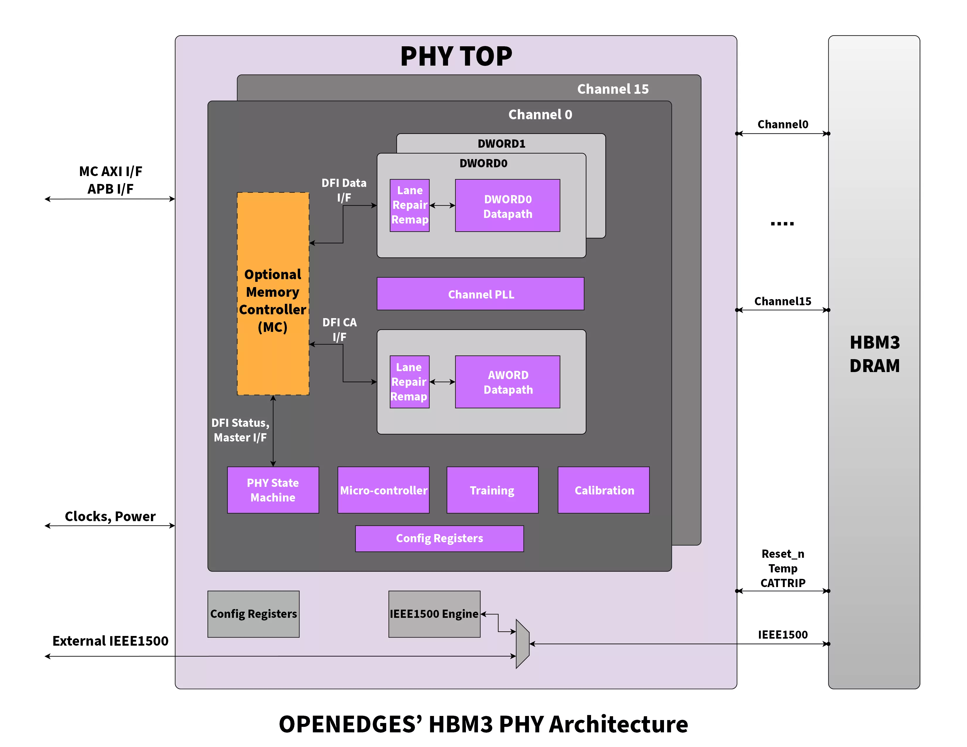
Block Diagram

Benefits

  • Configurability with Flexible Applications
    • Configurable channel and floor-plan allow connection to different DRAM package types and lane ordering
    • Minimal package substrate/PCB layer requirements enables PHY usage in low-cost applications
  • ​Performance
    • PSM enables accelerated firmware-based training
    • Ultra-fast fractional training
    • Programmable PHY boundary timing provides low read/write latency
  • Fast switching between FSPs
  • ​Capacity
    • Channel equalization and fast timing adjustment circuits enable 4 rank support to maximize capacity
  • ​Power
    • Power-saving modes with a variety of exit times
    • Multiple voltage domains to optimize voltage versus frequency

Applications

  • Provides an efficient solution for applications requiring high memory bandwidth, particularly in the fields of artificial Intelligence (AI), Machine Learning (ML), and general-purpose graphics processing units (GPGPU).

What’s Included?

  • Hard & Soft IP
    • GDSII, LEF, LVS, timing models, etc.
    • Verilog behavior models and encrypted RTL
    • Synthesis and STA constraints
    • Example test benches
  • Documentation
    • PHY Technical Reference Manual
    • Implementation, package, and PCB design guidelines
    • Test and characterization guidelines
    • Physical verification reports

Specifications

Identity

Part Number
OPHY_HBM3
Vendor
OPENEDGES Technology, Inc.
Type
Silicon IP
Controller / PHY
Controller + PHY , PHY

Files

Note: some files may require an NDA depending on provider policy.

Provider

Learn more about HBM IP core

Reducing Avoidable Memory Trips In HBM Systems

As AI and high-performance SoCs increasingly rely on HBM, memory bandwidth alone is no longer enough to maximize performance. This article discusses why the intelligent data movement and cache efficiency are critical to unlocking the full benefits of HBM-based architectures.

Making Strong Error-Correcting Codes Work Effectively for HBM in AI Inference

LLM inference is increasingly memory-bound, and HBM cost per GB now dominates system cost. Today’s HBM stacks include short on-die ECC, which tightens binning, raises price, and locks reliability policy inside the device. This paper asks a simple question: can we tolerate a much higher raw HBM bit error rate (BER) and still keep end-to-end correctness and throughput, without changing the HBM PHY or the fixed 32B transaction size?

High Bandwidth Memory Evolution from First Generation HBM to the Latest HBM4

HBM4 is the latest generation of the High Bandwidth Memory (HBM) that has become analogous to the Artificial Intelligence (AI) boom that is everywhere in today’s world. HBM is also increasingly being used in other applications like Data centers, autonomous driving systems, servers, cloud computing just to mention few domains where bandwidth and performance in a key requirement.

Breaking the HBM Bit Cost Barrier: Domain-Specific ECC for AI Inference Infrastructure

High-Bandwidth Memory (HBM) delivers exceptional bandwidth and energy efficiency for AI workloads, but its high cost per bit, driven in part by stringent on-die reliability requirements, poses a growing barrier to scalable deployment. This work explores a systemlevel approach to cost reduction by eliminating on-die ECC and shifting all fault management to the memory controller.

Frequently asked questions about HBM Interface IP

What is HBM3 PHY IP at 7/6nm?

HBM3 PHY IP at 7/6nm is a HBM IP core from OPENEDGES Technology, Inc. listed on Semi IP Hub.

How should engineers evaluate this HBM?

Engineers should review the overview, key features, supported foundries and nodes, maturity, deliverables, and provider information before shortlisting this HBM IP.

Can this semiconductor IP be compared with similar products?

Yes. Buyers can compare this product with similar semiconductor IP cores or IP families based on category, provider, process options, and structured technical specifications.

×
Semiconductor IP