High Bandwidth Memory 3 (HBM3/3E) IP optimized for Samsung SF4X
The HBM3 IP consists of a PHY and memory controller optimized for Samsung SF4X process to support the HBM3 memory standard (JESD2…
Overview
The HBM3 IP consists of a PHY and memory controller optimized for Samsung SF4X process to support the HBM3 memory standard (JESD238A) operating at up to 9.6 Gbps/pin. The HBM3 IP is designed for high memory throughput and low latency applications while minimizing area and power consumption.
Key features
- Supports up to 9.6 Gbps/pin
- Supports 16 channels (32 pseudo channels)
- Supports AXI4 mainband and AXI4-Lite sideband interfaces
- Supports up to 16H and up to 32Gb channel densities
- Supports Data Bus Inversion (DBI) signaling for lower power
- Memory controller with address remapping, out-of-order scheduling, anti-starvation and configurable page policies
- Native support for basic RAS features like command parity, ECS, RFM, ECC and data scrambling
- Supports static and dynamic clock gating
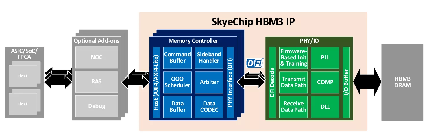
- Supports optional add-on blocks e.g., SkyeChip’s NOC as a switch for channel-interleaved system memory view
Block Diagram
Benefits
- Device Configuration Support: The HBM3 IP supports HBM3 and HBM3E DRAM die stacks of 4H, 8H, 12H and 16H. The HBM3 IP also supports up to 32Gb channel densities allowing interoperability with the HBM3 stack from any memory vendor. The PHY and memory controller is also fully covalidated for best performance and power on all 16 channels (32 pseudo channels) simultaneously.
- Memory Interface Training: The HBM3 PHY can operate independently to initialize and bring up the memory interface. To ensure the maximum channel timing margins, the PHY supports a myriad of interface training algorithms inclusive of command/address training and de-skew, read/write leveling, read/write data eye training with per-bit de-skew, DCD correction, VREF calibration and PVT tracking. The firmware-based initialization and training algorithms provide ultimate flexibility in accommodating future HBM3 specification updates and allow customizations for different memory vendors implementations.
- Design for Test/Debug/Manufacturing: The HBM3 PHY has an internal traffic generator that can test the memory interface independent of the memory controller with logical loopback mode to have the transmitted data to loopback on the receive path for test dan debug. It also supports all HBM3-defined test mechanisms including the IEEE1500 interface supporting DRAM repairs, DRAM BIST and interconnect redundancy remapping. In addition, it also supports other standard test and debug features like boundary scan, SRAM BIST and redundancy and scan.
Specifications
Identity
Provider
Learn more about HBM IP core
Making Strong Error-Correcting Codes Work Effectively for HBM in AI Inference
High Bandwidth Memory Evolution from First Generation HBM to the Latest HBM4
Breaking the HBM Bit Cost Barrier: Domain-Specific ECC for AI Inference Infrastructure
High Bandwidth Memory (HBM) at the AI Crossroads: Customization or Standardization?
Overcoming Timing Closure Issues in Wide Interface DDR, HBM and ONFI Subsystems
Frequently asked questions about HBM Interface IP
What is High Bandwidth Memory 3 (HBM3/3E) IP optimized for Samsung SF4X?
High Bandwidth Memory 3 (HBM3/3E) IP optimized for Samsung SF4X is a HBM IP core from SkyeChip listed on Semi IP Hub.
How should engineers evaluate this HBM?
Engineers should review the overview, key features, supported foundries and nodes, maturity, deliverables, and provider information before shortlisting this HBM IP.
Can this semiconductor IP be compared with similar products?
Yes. Buyers can compare this product with similar semiconductor IP cores or IP families based on category, provider, process options, and structured technical specifications.