HBM2E PHY V2 (Hard 1) - TSMC 7FF18
graphics, high-performance computing (HPC) and networking applications are requiring more memory bandwidth to keep pace with the …
Overview
Advanced graphics, high-performance computing (HPC) and networking applications are requiring more memory bandwidth to keep pace with the increasing compute performance brought by advanced process technologies. With the HBM2/HBM2E IP solution, designers can achieve their memory throughput requirements with minimal power consumption and low latency.
The complete HBM2/HBM2E IP solution includes controller, PHY and verification IP, enabling designers to achieve up to 460 GBps aggregate bandwidth, which is over 14 times the bandwidth of a 72-bit DDR4 interface operating at up to 3200 Mbps. In addition, the HBM2/HBM2E IP solution delivers approximately 10X better energy efficiency than DDR4.
The HBM2/HBM2E IP solution leverages elements from the silicon-proven DDR4 IP, which has been validated in hundreds of designs and shipped in millions of systems-on-chips (SoCs), enabling designers to lower integration risk and accelerate adoption of the new standard. In addition, the HBM IP is in volume production with numerous customer SoCs.
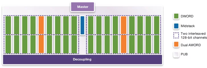
The HBM2/HBM2E PHY is provided as a set of hard macrocells delivered as GDSII along with a soft PHY Utility Block (PUB). The hard macrocells include integrated application-specific HBM2/HBM2E I/Os required for HBM2/HBM2E signaling and are easily assembled into a complete 512- or 1,024-bit HBM2/HBM2E PHY. The PUB provides the PHY configuration registers, training algorithms, and BIST features of the interface. The design is optimized for high performance, low latency, low area, low power, and ease of integration.
In select process technologies, the vendor also offers pre-hardened HBM2/HBM2E PHY options. For designers with unique requirements, the vendor also offers services to harden a DDR/HBM PHY to meet exact target requirements including metal stack, decoupling parameters, etc.
Key features
- Complete HBM2/HBM2E IP solution, including PHY, controller and verification IP, reduces integration risk while minimizing time-to-market
- 2.5D interposer expertise and reference designs
- Supports 2.5D-based JEDEC standard HBM2/HBM2E SDRAMs with data rates up to 3200 Mbps
- Up to 2400 Mbps with HBM2
- Up to 3600 Mbps with HBM2E
- Pseudo-channel mode doubles the number of channels, resulting in smaller fetch size and higher performance
- The HBM2/HBM2E IP is based on Synopsys’ silicon-proven HBM and DDR4 IP that has been integrated into hundreds of SoC designs
- DFI 4.0-compatible interface
- PHY independent training capability
- Comprehensive set of design-for-test (DFT) features
Block Diagram
Silicon Options
| Foundry | Node | Process | Maturity |
|---|---|---|---|
| TSMC | 7nm | N7FF | — |
Specifications
Identity
Files
Note: some files may require an NDA depending on provider policy.
Provider
Learn more about HBM IP core
AMD GPUs using new HBM DRAM (and the cost/benefit appears balanced!)
HBM Performance Verification Made Easy
Arm and Synopsys: Delivering an Integrated, Nine-Stage “Silicon-to-System” Chip Design Flow
Synopsys Interconnect IPs Enabling Scalable Compute Clusters
High-Speed Test IO: Addressing High-Performance Data Transmission And Testing Needs For HPC & AI
Frequently asked questions about HBM Interface IP
What is HBM2E PHY V2 (Hard 1) - TSMC 7FF18?
HBM2E PHY V2 (Hard 1) - TSMC 7FF18 is a HBM IP core from Synopsys, Inc. listed on Semi IP Hub. It is listed with support for tsmc.
How should engineers evaluate this HBM?
Engineers should review the overview, key features, supported foundries and nodes, maturity, deliverables, and provider information before shortlisting this HBM IP.
Can this semiconductor IP be compared with similar products?
Yes. Buyers can compare this product with similar semiconductor IP cores or IP families based on category, provider, process options, and structured technical specifications.