Overview
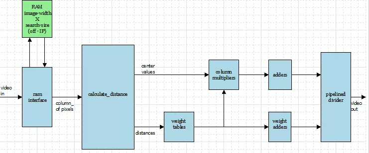
NLM (Non Local Mean) is a noise reduction algorithm wherein the value of each pixel is determined a rectangle of pixels around that pixel (a “center patch”) with all identically-sized rectangles of pixels (“search patches”) within a relatively large rectangle around the pixel (the “search window”). A weight is then given to the center pixel of each “search patch” according to the distance of the corresponding search patch from the center patch, and the output pixel is derived by calculating the weighted average of all the pixels in the search window.
This algorithm is relatively complex, requiring a large number of gates. VLSI Plus V-NLM-01 product, however, significantly reduces the number of gates by performing two operations in each clock cycle, keeping an energy efficient architecture where consecutive operations are done on neighboring pixels.
Learn more about Video Processing IP core
The imbalance between I/O speed and internal logic speed in integrated circuits has shifted in recent years in favor of the I/O. While in the past, the performance of integrated circuits was often limited by the I/O rate, today, in both ASICs and FPGAs, internal logic struggles to keep up with the I/O performance.
In this article, we show how fast video streams conforming to MIPI CSI2 rev2.0 over MIPI DPHY rev1.2 can be generated, using VLSI Plus’ SVTPlus-CSI2-F IP core, with simple off-FPGA analog front-end. The high bit rates can be achieved with a relatively slow FPGA clock frequency, trading off FPGA resources for simple timing closure.
VLSI Plus today announced the availability of the CSI2-MUX-A1-F – a MIPI® CSI2 transceiver, connecting to up to 4 CSI2 camera inputs, and outputting a multiplexed CSI2 stream with 4 data lanes, at up to 1.5Gbps per lane.
VLSI Plus today announced at the MWC conference the availability of the SVT-CS4-AP2 – a MIPI® CSI2 compliant serial video transmitter, supporting multiple concurrent video sources, and employing from 1 to 4 DPHY lanes at up to 1.5Gbps per lane.
VLSI Plus today announced the availability of Alias-DT option, which enables outputting multiple pixels per clock, in all its MIPI® CSI2 Receiver IP cores (the SVR family).
VLSI Plus today announced the availability of the SVRPlus-CSI2-F a 64 bit serial video receiver, supporting MIPI® CSI2 and extensions to CSI2 with up to 8 data lanes and two clock lanes, and outputting 1, 2 or 4 pixels per clock.