Vendor: SmartDV Category: GDDR

GDDR7 Memory Model

GDDR7 Memory Model provides an smart way to verify the GDDR7 component of a SOC or a ASIC.

Overview

GDDR7 Memory Model provides an smart way to verify the GDDR7 component of a SOC or a ASIC. The SmartDV's GDDR7 memory model is fully compliant with draft GDDR7 JEDEC Specification and provides the following features. Better than Denali Memory Models.

GDDR7 Memory Model is supported natively in SystemVerilog, VMM, RVM, AVM, OVM, UVM, Verilog, SystemC, VERA, Specman E and non-standard verification env

GDDR7 Memory Model comes with optional Smart Visual Protocol Debugger (Smart ViPDebug), which is GUI based debugger to speed up debugging.

Key features

  • Supports GDDR7 memory devices from all leading vendors.
  • Supports 100% of GDDR7 protocol draft JEDEC specification.
  • Supports all the GDDR7 commands as per the specs.
  • Supports 4 separate independent channels with point-to-point interface for data, address and command.
  • Supports command parity
  • Supports Double Data Rate (DDR)
  • Supports Pseudo channel mode operation.
  • Supports 16 - 64 Gbit densities
  • Supports X8 mode.
  • Supports RDQS Mode.
  • Supports DQ preamble.
  • Supports Bank group features.
  • Supports Programmable Read/Write latency.
  • Supports Bank grouping and 16 internal banks per channel.
  • Supports Data bus inversion (DBI) & Command Address bus inversion (CABI).
  • Supports Read/Write data transmission integrity secured by cyclic redundancy check.
  • Supports ECC.
  • Supports Input/output PLL/DLL on/off mode.
  • Supports Read/Write EDC on/off mode.
  • Supports Programmable EDC hold pattern for CDR.
  • Supports Programmable CRC Read/Write latency.
  • Supports Low Power modes.
  • Supports Auto refresh & self-refresh modes.
  • Supports On-die termination operation.
  • Supports Command Address, WCK2CK, Read and Write Training mode’s.
  • Supports IEEE.1149.1 boundary scan operation.
  • Checks for following
    • Check-points include power on, Initialization and power off rules,
    • State based rules, Active Command rules,
    • Read/Write Command rules etc.
    • All timing violations.
  • Supports callbacks for user to get command data on bus.
  • Supports all mode registers programming.
  • Supports for power down features.
  • Supports for input clock stop and frequency change.
  • Quickly validates the implementation of the draft GDDR7 protocol JEDEC specification.
  • Bus-accurate timing for min, max and typical values.
  • Constantly monitors GDDR7 behavior during simulation.
  • Protocol checker fully compliant with GDDR7 draft JEDEC specification.
  • Notifies the test bench of significant events such as transactions, warnings, timing and protocol violations.
  • Built in functional coverage analysis.
  • Supports Callbacks, so that user can access the data observed by monitor.

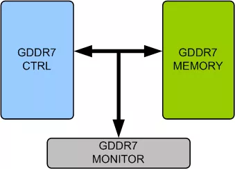
Block Diagram

Benefits

  • Faster testbench development and more complete verification of GDDR7 designs.
  • Easy to use command interface simplifies monitor control and configuration.
  • Simplifies results analysis.
  • Runs in every major simulation environment.

What’s Included?

  • Complete regression suite containing all the GDDR7 testcases.
  • Examples showing how to connect and usage of Model.
  • Detailed documentation of all class, task and function's used in verification env.
  • Documentation also contains User's Guide and Release notes.

Specifications

Identity

Part Number
GDDR7 Memory Model
Vendor
SmartDV
Type
Silicon IP
Controller / PHY
Controller

Files

Note: some files may require an NDA depending on provider policy.

Provider

HQ: India

Learn more about GDDR IP core

Keeping Pace with CXL Specification Revisions

As the Compute Express Link® (CXL®) specification rapidly evolves, so too must the tools and infrastructure used to verify designs built around it. Maintaining verification IP (VIP) that keeps pace with new specification revisions is no small task, particularly when dealing with major version shifts like the transition from CXL 2.0 to 3.0.

SmartDV Licenses SDIO IP Family to Ranix for V2X Products

To meet RANiX’s unique design goals, SmartDV will customize the IP to go beyond the standard SDIO functionality—thereby empowering RANiX to differentiate from their competitors. SmartDV will also provide RANiX with the requisite support and documentation to achieve ASIL certification for ISO 26262.

SmartDV Rolls Out Multi-Phase Expansion Plan

SmartDV™ Technologies, provider of flexible, customizable semiconductor design IP (intellectual property) and verification solutions, has expanded engineering operations beyond its headquarters in Bengaluru with the opening of a new office space in Coimbatore, Tamil Nadu, India.

Frequently asked questions about GDDR Interface IP

What is GDDR7 Memory Model?

GDDR7 Memory Model is a GDDR IP core from SmartDV listed on Semi IP Hub.

How should engineers evaluate this GDDR?

Engineers should review the overview, key features, supported foundries and nodes, maturity, deliverables, and provider information before shortlisting this GDDR IP.

Can this semiconductor IP be compared with similar products?

Yes. Buyers can compare this product with similar semiconductor IP cores or IP families based on category, provider, process options, and structured technical specifications.

×
Semiconductor IP