Vendor: SmartDV Technologies Category: I2C / I3C

AVSBus Verification IP

AVSBus Verification IP provides a smart way to verify the AVSBus (Adaptive Voltage Scaling) component of a SOC or a ASIC.

Verification IP View all specifications

Overview

AVSBus Verification IP provides a smart way to verify the AVSBus (Adaptive Voltage Scaling) component of a SOC or a ASIC. The SmartDV's AVSBus Verification IP is fully compliant with standard PMBus 1.3.1 Part III Specification and provides the following features.

AVSBus Verification IP is supported natively in SystemVerilog, VMM, RVM, AVM, OVM, UVM, Verilog, SystemC, VERA, Specman E and non-standard verification env

AVSBus Verification IP comes with optional Smart Visual Protocol Debugger (Smart ViPDebug), which is GUI based debugger to speed up debugging.

Key features

  • Follows AVSBUS specification as defined in PMBus version 1.3.1 Part III Specification.
  • Supports data width up to 64 bits.
  • Support AVSBus Master and Slave Functionality.
  • Supports 3-wire, 2-wire AVSBus interface.
  • Supports all AVSBus Commands as per specs.
  • Supports Clock Resynchronization.
  • Support timeout detection and generation.
  • Supports Master Alert Generation.
  • Supports back to back commands.
  • Supports user response frame.
  • Supports Clock Suspension.
  • Supports following AVSBus topologies
  • o Single Master and Single Slave.
  • o Multiple links.
  • Supports Frame Alignment.
  • Supports insertion of various errors
    • Start code error
    • CRC error
    • Selector error
    • Command type error
    • Command group error
    • Command data type error
    • Unavailable Resource error
    • Invalid reserved bit error
    • Invalid values on SDATA and MDATA when clock suspension error
  • Built in functional coverage analysis.
  • Supports Callbacks in Master, Slave and Monitor for modifying and sampling data/command on AVSBus.
  • Notifies the test bench of significant events such as transactions, warnings and protocol violations. This can be written to separate log files.
  • AVSBus Verification IP comes with complete testsuite to test every feature of AVSBus specification.

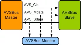
Block Diagram

Benefits

  • Faster testbench development and more complete verification of AVSBus designs.
  • Easy to use command interface simplifies testbench control and configuration of slave and master.
  • Simplifies results analysis.
  • Runs in every major simulation environment.

What’s Included?

  • Complete regression suite containing all the AVSBus testcases.
  • Examples showing how to connect various components, and usage of Master, Slave and Monitor.
  • Detailed documentation of all class, task and function's used in verification env.
  • Documentation contains User's Guide and Release notes.

Specifications

Identity

Part Number
AVSBus VIP
Vendor
SmartDV Technologies
Type
Verification IP

Files

Note: some files may require an NDA depending on provider policy.

Provider

Learn more about I2C / I3C IP core

From I2C to I3C: Evolution of Two-Wire Communication in Embedded Systems

The I2C (Inter-Integrated Circuit) Bus invented in 1980 by Philips Semiconductors (NXP Semiconductors today) was a massive step forward in simplifying communications in embedded systems. It is a simple two-wire interface for synchronous, multi-master/multi-slave, single ended serial communication. Fast forward 45 years to today and it is still widely used for attaching low speed peripheral Integrated Circuits (ICs), processors and microcontrollers. But silicon today has changed...

Maximizing the Usability of Your Chip Development: Design with Flexibility for the Future

Early in my career selling chips for Motorola Semiconductor, the ability to spin derivative microcontroller chips for a customer’s specific requirement was relatively straightforward. If the volume looked reasonable, we would tape-out a new chip with a few added features because mask costs and wafers were relatively inexpensive at the larger process nodes. The customer won by getting an MCU tailored to their specific need, and Motorola won by gaining a more committed customer plus another SKU that could be sold to other customers – boosting ROI. With the migration to higher cost FinFET nodes, those times are long gone as the economics no longer work.

MIPI CCI over I3C: Faster Camera Control for SoC Architects

Imagine a camera subsystem that responds in microseconds, consumes less power, and offers a more straightforward route to time-to-market. For SoC architects and IP integration teams, that vision is increasingly possible with MIPI Camera Control Interface (CCI) over I3C.

Frequently asked questions about I2C / I3C IP cores

What is AVSBus Verification IP?

AVSBus Verification IP is a I2C / I3C IP core from SmartDV Technologies listed on Semi IP Hub.

How should engineers evaluate this I2C / I3C?

Engineers should review the overview, key features, supported foundries and nodes, maturity, deliverables, and provider information before shortlisting this I2C / I3C IP.

Can this semiconductor IP be compared with similar products?

Yes. Buyers can compare this product with similar semiconductor IP cores or IP families based on category, provider, process options, and structured technical specifications.

×
Semiconductor IP