Overview
The Analog TV Demodulator and Decoder IP core is extracted from a production chip and a silicon-proven IP core. The Analog TV demodulator and decoder are two separate blocks of IP cores available as a single license. The input to the demodulator is digital I/Q LIF or Baseband, the input sample rate is customizable to meet the ADC requirement.
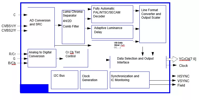
The Analog TV Decoder IP contains a high-quality front-end video circuit for processing all analog NTSC/PAL/SECAM standards into a 4:2:2 YCrCb digital video format as well as conventional analog RGB or YCrCb signals. The programmable through an I²C interface.
The provides a cost-effective solution for digitized TV, LCD TV/monitors, digital TV, STB, video surveillance security, video conferencing, video capturing devices, and PC video card.
The Analog TV Demodulator IP provides support for PAL, NTSC, and SECAM. The all-digital implementation is suitable for integration into digital demodulators and digital SOC devices. The solution covers worldwide TV standards, this IP core block also extracted from production SOC.
The input to the demodulator is digital I/Q at baseband at a 19.33 Msps sample rate. The input sample rate is customizable to meet the requirement and changes to the sample rate will require modifications to the filter chain.
For supporting an IF input, the IF frequency is customizable to meet the requirement. For IF inputs, phase rotation to baseband is accomplished by the “Freq correction” block at left using direct digital frequency synthesis (DDFS).
Learn more about Modulation Demodulation IP core
T2M-IP, the global leader in semiconductor IP cores and technology expertise, is proud to announce the immediate availability of its partner's VESA-compliant DisplayPort v1.4 Rx PHY and Controller IP Cores.
T2M announces the availability of its partner’s Bluetooth V6.0 RF Transceiver IP Core in 22nm ULL and 40nm ULP.
Incorporating BroadR-Reach™ technology for Automotive Excellence, this PHY delivers exceptional performance for automotive and industrial applications, providing a superior alternative to traditional BaseT1 solutions.
Designed to meet the evolving needs of next-generation automotive and industrial applications, the CAN XL Controller IP offers superior performance and flexibility while maintaining backward compatibility with previous CAN standards.
T2MIP, a leading provider of semiconductor IP cores, proudly announces the immediate availability of their partner's H.264 and H.265 HEVC Codec IP cores.
T2M-IP is excited to announce that its state-of-the-art USB 3.0 IP, developed in the 22nm ULP (Ultra Low Power) and ULL (Ultra Low Leakage) process technologies, has been successfully licensed to over 10 customers worldwide in the past two years.