Vendor: Cadence Design Systems, Inc. Category: DSP Core

Next-generation DSP for embedded vision and AI with millions of units shipped in the market

First DSP for embedded vision and AI with millions of units shipped in the market The Cadence® Tensilica® Vision P6 DSP, introduc…

Overview

512-bit SIMD Vision DSPs for Camera, Radar, and AI

The Cadence® Tensilica® Vision 130 is the successor to the Vision P6 DSP, introduced in 2016. Vision 130 DSP is developed for the newly introduced Tensilca Xtensa LX8 controller. Vision 130 offers the best energy efficiency while offering the performance required for Imaging, Computer Vision, Radar, and AI with its 512-bit SIMD.

Key features

Cadence, through its Tensilica processor IP, brings together best-in-class products and services from industry leaders to help you accelerate the development of your SoC designs while meeting your demanding power and performance requirements. Browse the list of Tensilica processor IP service partners below.

  • 1024/512b Load/Store capabilities
  • 256 8-bit MAC
  • 8/16/32-bit fixed-point processing
  • Single-precision (FP32) and half-precision (FP16) floating-point processing
  • Integrated 3D iDMA
  • User-defined instructions support
  • Built on LX8 Xtensa processor offering best energy efficiency
  • ISO 26262 ready for automotive market

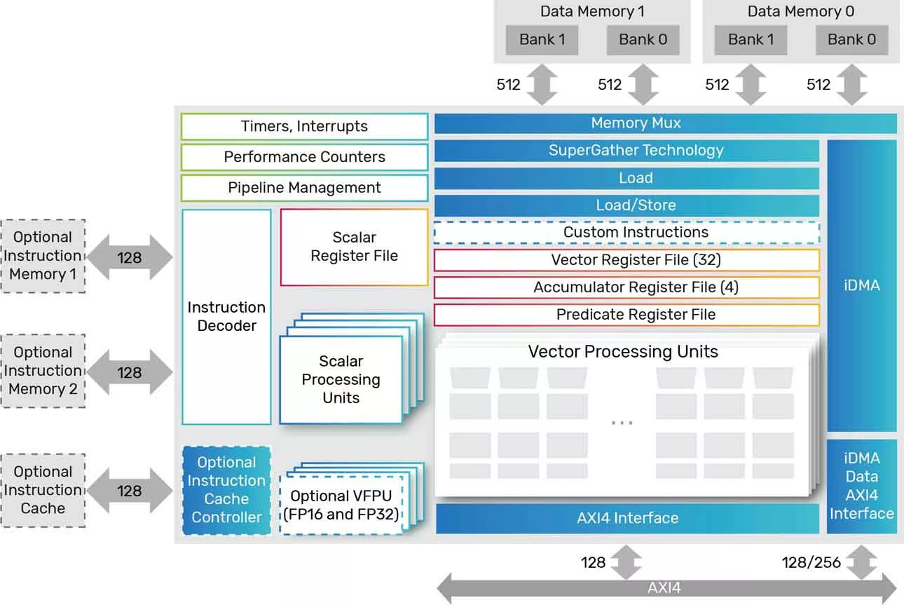
Block Diagram

Benefits

Energy Efficient

Low power compared to host CPU and GPU

Vision/Image Processing

Instruction set optimized for computer vision and image processing applications

High Performance

> 1TOPS AI performance for object detection, image classification, image segmentation

Specifications

Identity

Part Number
Vision 130 DSP
Vendor
Cadence Design Systems, Inc.
Type
Silicon IP

Files

Note: some files may require an NDA depending on provider policy.

Provider

Learn more about DSP Core IP core

How a Multi-Protocol PHY Simplifies Physical AI Connectivity

Physical AI systems must move large amounts of data across two very different connectivity domains. Accelerators and local storage need high-bandwidth, low-latency links close to the compute SoC, while sensors and control modules require reliable connectivity across the larger platform. Supporting both domains with separate high-speed PHYs can increase silicon area and integration complexity.

Frequently asked questions about DSP Core IP cores

What is Next-generation DSP for embedded vision and AI with millions of units shipped in the market?

Next-generation DSP for embedded vision and AI with millions of units shipped in the market is a DSP Core IP core from Cadence Design Systems, Inc. listed on Semi IP Hub.

How should engineers evaluate this DSP Core?

Engineers should review the overview, key features, supported foundries and nodes, maturity, deliverables, and provider information before shortlisting this DSP Core IP.

Can this semiconductor IP be compared with similar products?

Yes. Buyers can compare this product with similar semiconductor IP cores or IP families based on category, provider, process options, and structured technical specifications.

×
Semiconductor IP