ONFI 5.2: What’s new in Open NAND Flash Interface's latest 5.2 standard
ONFI 5.2 is the latest generation of ONFI device standard, published in 2024. ONFI 5.2 devices have added several major features over previous generation ONFI standards.
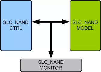
SLC NAND Memory Model provides an smart way to verify the SLC NAND component of a SOC or a ASIC.
SLC NAND Memory Model provides an smart way to verify the SLC NAND component of a SOC or a ASIC. The SmartDV's SLC NAND memory model is fully compliant with standard SLC NAND Specification and provides the following features. Better than Denali Memory Models.
SLC NAND Memory Model is supported natively in SystemVerilog, VMM, RVM, AVM, OVM, UVM, Verilog, SystemC, VERA, Specman E and non-standard verification env
SLC NAND Memory Model comes with optional Smart Visual Protocol Debugger (Smart ViPDebug), which is GUI based debugger to speed up debugging.
Note: some files may require an NDA depending on provider policy.

SLC NAND Memory Model is a NAND Flash IP core from SmartDV Technologies listed on Semi IP Hub.
Engineers should review the overview, key features, supported foundries and nodes, maturity, deliverables, and provider information before shortlisting this NAND Flash IP.
Yes. Buyers can compare this product with similar semiconductor IP cores or IP families based on category, provider, process options, and structured technical specifications.