Vendor: Arasan Chip Systems Inc. Category: NAND Flash

ONFI 4.2 NAND Flash Software Driver

The NAND Flash landscape is changing and the Arasan NAND Flash Controller IP Core is changing in accordance with it.

Overview

The NAND Flash landscape is changing and the Arasan NAND Flash Controller IP Core is changing in accordance with it. New applications are emerging and innovative IP solutions are needed to keep pace. NAND Flash is being incorporated into all types of products including Portable memory drives, Media players, Digital cameras, Smartphones, eBook Readers, Tablets, Digital TVs, Digital camcorders, PCs, and so on. Arasan is in the perfect position to give you what you need.

The NAND Flash Controller IP Core is a full-featured, easy to use, synthesizable core, easily integrated into any SoC or FPGA development. Designed to support SLC, MLC and TLC flash memories, it is flexible in use and easy in implementation. The controller works with any suitable NAND Flash memory device up to 1024Gb from leading memory providers – Micron, Samsung, Toshiba and Hynix. The IP core includes a host of configuration options from page size to bank selects. The controller offers BCH Error Code Correction (ECC), with options for either correcting 4b, 8b, 12b, or 16b per 512 Bytes, or 24b, 32b, or even 60b per 1024 Bytes, for long term reliability.

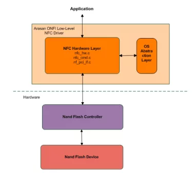
The IP core supports the Open NAND Flash Interface Working Group (ONFI) 4.2 standards. The design has been built around a modern bus architecture, supporting both AXI3 and AXI4.  Bridges may be used to provide support for other host bus interfaces if required. The slave AXI IP supports an external DMA interface where the master AXI incorporates an internal DMA controller.

The Arasan NAND Flash Controller IP Cores are delivered in Verilog RTL that can be implemented in an ASIC or FPGA. They are fully tested with vendor models and hardware is tested with FPGA’s. The core includes RTL code, test scripts and a test environment for complete simulation and verification.

NAND Flash Interface

Arasan Chip System’s NAND flash controller IP provides easy, reliable access to an off-chip NAND flash. It is backwards compatible, supporting the Single Data Rate (asynchronous) mode, the original Double Data Rate (synchronous) mode, as well as the newest and highest speed NVDDR3 mode. All data rates from all modes are supported.

The IP consists of two primary components: a host controller and a high speed PHY. The host controller is controlled via an AXI slave port. A scatter/gather DMA provides a separate AXI master port, allowing for extended unattended reads or writes. The host controller supports either AXI3 or AXI4, and a user configurable data path width.

AXI Control Interface

The primary interface to the ONFI controller is an AXI slave interface.  This is a full AXI interface, whether AXIv3 or AXIv4, offering access to both control registers and an external SRAM staging area.  The staging area is used to make sure transfers never need to be interrupted, either when reading or writing to the flash, and it supports high speed AXI bus access such as might be used by either the internal DMA or an external DMA.  The AXI data width is also fully configurable, allowing the user better control of any area versus throughput tradeoffs when transferring to and from the host environment.

AXI DMA Interface

An integrated DMA controller provides for a hands-off, memory-copy like interface.  This can be used to transfer data to or from the device at high speed.  Moreover, the DMA supports a parallelism option, allowing transfers to automatically be parallelized to the various hardware components in an ONFI device.

This support has been simplified to the level of a CPU memory copy request, requiring a bare minimum of software to transfer small or large amounts of data to or from the flash.  Indeed, this parallelization feature can massively improve the throughput of any DMA transfer.

Key features

  • ONFI v 4.2 compliant
    • Supports all specified transfer rates, from 10MB/s all the way up to 1.6GB/s
  • All I/O modes supported
    • SDR (Asynchronous mode)
    • NVDDR (. Synchronous mode)
    • NVDDR2/3
  • Configurable AXI ports
    • AXI3 or AXI4
    • 32b – 1024b bus widths
  • AXI DMA master
    • Scatter / Gather
    • Parameterized width
    • Max Bus Throughput
  • PHY BIST support
  • Support Radiation hardening [defence, space, nuclear applications etc.]
  • Separate command processors
    • Creates and maximizes parallelism across host targets
    • Arasan’s unique parallelism algorithm can speed up read and write operations by up to 32x.
    • Once configured, cross-channel parallelism is accomplished seamlessly and automatically.
    • Parallel commands are automatically generated via the DMA
  • Integrated scrambler
    • Can be configured to automatically scramble data pages on read and write, sufficient to meet the scrambling requirements of modern flash devices.
    • Scrambler size, algorithm, and polynomial are all user configurable parameters
  • BCH code support
    • Provides automatic BCH parity generation, and ECC decoding.
    • BCH ECC size and support may be either run-time configured, or fixed at synthesis time, allowing the user better area/performance tradeoffs.
    • ECC operations may either be duplicated across data paths, for greater throughput, or shared across data paths for better area performance.
  • CRC feature
    • An optional CRC check may be applied to each BCH parity block, for additional error detection capability.
    • Both the CRC size and polynomial may be user configured.


ONFI 4.2 PHY

  • Compliant to ONFI specification version 4.2
  • Supports NV-DDR3 mode of operation supporting up to 800MHz
  • Supports NV-DDR2 mode of operation supporting up to 400MHz
  • Supports NV-DDR mode of operation supporting up to 100MHz
  • Supports legacy Asynchronous devices operating from 10MHz to 50MHz
  • Can be used with Arasan’s ONFI 4.2 NAND Flash Controller IP
  • Supports 1.2V & 1.8V operation I/O pads
  • Supports both DQS and DAT launch and return alignment with 78ps resolution
  • Return signal phase alignment keeps the IP working across PVT variations
  • Supports up to +/-200ps of bit level deskew on READ and WRITE
  • Supports differential signaling of DQS and RE signals
  • Supports four levels of drive strength as mentioned in the ONFI 4.2 standard
  • Supports Manufacturability tests – DC SCAN and ABIST

Block Diagram

Files

Note: some files may require an NDA depending on provider policy.

Specifications

Identity

Part Number
ONFI 4.2 NAND FLASH SOFTWARE DRIVER
Vendor
Arasan Chip Systems Inc.

Provider

Arasan Chip Systems Inc.
HQ: USA
Arasan Chip Systems, is a leading provider of IP for mobile storage and mobile connectivity interfaces with over a billion chips shipped with our IP. Arasan’s high-quality, silicon-proven, Total IP Solutions include digital IP, Analog Mixed Signal PHY IP, Verification IP, HDK, and Software. Arasan has a focused product portfolio targeting mobile SoCs. The term Mobile has evolved over our two-decade history to include all things mobile – starting with PDA’s in the mid 90’s to smartphones to today’s Automobiles, Drones, and IoT. Arasan is at the forefront of this evolution of “Mobile” with its standards-based IP at the heart of Mobile SoCs.

Learn more about NAND Flash IP core

The Future of Storage: From eMMC to the Blazing Speeds of UFS 5.0

In the world of mobile and embedded electronics, storage is no longer just about capacity; it’s about how fast that data can move. As we transition into an era of on-device AI and 8K video, the standards we rely on—UFS, eMMC, and NAND—are evolving rapidly.

Universal Flash Storage: Mobilize Your Data

Universal Flash Storage (UFS) was created for mobile applications and computer systems requiring high performance and low power consumption. These systems typically use embedded Flash based on the JEDEC standard eMMC. UFS was defined by JEDEC as the evolutionary replacement for eMMC offering significantly higher memory bandwidth. The standard builds on existing standards such as the SCSI command set, the MIPI Alliance M-PHY and UniProSM as well as eMMC form factors to simplify adoption and development.

Arasan’s xSPI/eMMC5.1 PHY: Unified Dual-Mode Physical Layer IP

As SoCs evolve to support a growing range of memory interfaces, designers are faced with the challenge of balancing integration complexity, pin efficiency, and performance scalability. Traditionally, implementing both xSPI (JESD251) for boot and eMMC 5.1 for high-speed storage required separate PHYs, leading to increased silicon area, power consumption, and I/O overhead.

UFS Goes Mainstream

UniversalFlash Storage (UFS) was created for mobile applications and computer systems requiring high performance and low power consumption. These systems typically use embedded Flash based on the JEDEC standard eMMC. UFS was defined by JEDEC as the evolutionary replacement for eMMC offering significantly higher memory bandwidth. The standard builds on existing standards such as the SCSI command set, the MIPI Alliance M-PHY and UniPro as well as eMMC form factors to simplify adoption and development.

Frequently asked questions about NAND Flash IP

What is ONFI 4.2 NAND Flash Software Driver?

ONFI 4.2 NAND Flash Software Driver is a NAND Flash IP core from Arasan Chip Systems Inc. listed on Semi IP Hub.

How should engineers evaluate this NAND Flash?

Engineers should review the overview, key features, supported foundries and nodes, maturity, deliverables, and provider information before shortlisting this NAND Flash IP.

Can this semiconductor IP be compared with similar products?

Yes. Buyers can compare this product with similar semiconductor IP cores or IP families based on category, provider, process options, and structured technical specifications.

×
Semiconductor IP