Overview
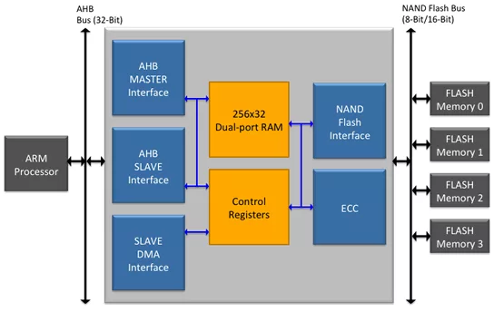
The ONFI 2.3 NAND Flash Controller IP Core is a full-featured, easy to use, synthesizable core, easily integrated into any SoC or FPGA development. Designed to support both SLC and MLC flash memories, ONFI 2.3 NAND controller IP is flexible in use and easy in implementation. The controller works with any suitable NAND Flash memory device up to 128 Gb from leading memory providers – Micron, Samsung, Toshiba and Hynix. The IP core includes a host of configuration options from page size to band selects. The controller offers Hamming Code (1-Bit error correction and 2-Bit error detection) and BCH (option for 4-, 8-, 12-, up to 32-Bit error correction) error code correction (ECC) for optimized performance and reliability. Additional features include the capability to boot from flash.
ONFI2.3 NAND Controller IP core supports the Open NAND Flash Interface Working Group (ONFI) 1.0, 2.0, 2.1, 2.2 and 2.3 standards and the Micron ClearNAND. It can also support a variety of host bus interfaces for easy adoption into any design architecture – AHB, APB, OCP, 8051 or custom buses. The slave AHB IP supports an external DMA interface where the master AHB incorporates an internal DMA controller.
An optional NAND Flash File system is available to support advanced features. The file system converts complicated tasks of NAND flash memory interfacing to simple memory access. Flash memory read, write, garbage collection, bad block management and other functions are handled in the background by the file system.
Learn more about NAND Flash IP core
NAND FLASH memories are non-volatile, inexpensive and of high capacity. These characteristics make these devices ideal for fulfilling the storage requirements in the exploding mobile device market.
In the world of mobile and embedded electronics, storage is no longer just about capacity; it’s about how fast that data can move. As we transition into an era of on-device AI and 8K video, the standards we rely on—UFS, eMMC, and NAND—are evolving rapidly.
Universal Flash Storage (UFS) was created for mobile applications and computer systems requiring high performance and low power consumption. These systems typically use embedded Flash based on the JEDEC standard eMMC. UFS was defined by JEDEC as the evolutionary replacement for eMMC offering significantly higher memory bandwidth. The standard builds on existing standards such as the SCSI command set, the MIPI Alliance M-PHY and UniProSM as well as eMMC form factors to simplify adoption and development.
As SoCs evolve to support a growing range of memory interfaces, designers are faced with the challenge of balancing integration complexity, pin efficiency, and performance scalability. Traditionally, implementing both xSPI (JESD251) for boot and eMMC 5.1 for high-speed storage required separate PHYs, leading to increased silicon area, power consumption, and I/O overhead.
UniversalFlash Storage (UFS) was created for mobile applications and computer systems requiring high performance and low power consumption. These systems typically use embedded Flash based on the JEDEC standard eMMC. UFS was defined by JEDEC as the evolutionary replacement for eMMC offering significantly higher memory bandwidth. The standard builds on existing standards such as the SCSI command set, the MIPI Alliance M-PHY and UniPro as well as eMMC form factors to simplify adoption and development.
ONFI 5.2 is the latest generation of ONFI device standard, published in 2024. ONFI 5.2 devices have added several major features over previous generation ONFI standards.