Overview
The NAND flash controller IP provides easy, reliable access to an off-chip NAND flash. It supports all modes of the Open NAND Flash Interface (ONFI) Specification, revision 5.0, release candidate 0.5, dated 1 March 2021. It is backwards compatible, supporting the Single Data Rate (asynchronous) mode, the double data rate moves NV-DDR, NV-DDR2, and NVDDR3, to include the latest NV-LPDDR4 recently introduced in the latest revision. All posted rates for these various modes are also supported, from the NV-DDR 33MHz mode at the low end all the way up to the newer 1,200MHz (2.4GT/s) I/O speeds.
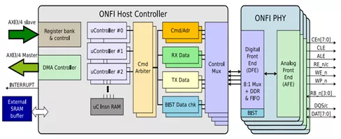
The IP consists of two primary components: a host controller and two or more high speed PHY interface controllers. The host controller is controlled via an AXI slave port. A scatter/gather DMA provides a separate AXI master port, allowing for extended unattended reads or writes. The host controller supports either AXI3 or AXI4, and a user configurable data path width.
Learn more about NAND Flash IP core
NAND FLASH memories are non-volatile, inexpensive and of high capacity. These characteristics make these devices ideal for fulfilling the storage requirements in the exploding mobile device market.
In the world of mobile and embedded electronics, storage is no longer just about capacity; it’s about how fast that data can move. As we transition into an era of on-device AI and 8K video, the standards we rely on—UFS, eMMC, and NAND—are evolving rapidly.
Universal Flash Storage (UFS) was created for mobile applications and computer systems requiring high performance and low power consumption. These systems typically use embedded Flash based on the JEDEC standard eMMC. UFS was defined by JEDEC as the evolutionary replacement for eMMC offering significantly higher memory bandwidth. The standard builds on existing standards such as the SCSI command set, the MIPI Alliance M-PHY and UniProSM as well as eMMC form factors to simplify adoption and development.
As SoCs evolve to support a growing range of memory interfaces, designers are faced with the challenge of balancing integration complexity, pin efficiency, and performance scalability. Traditionally, implementing both xSPI (JESD251) for boot and eMMC 5.1 for high-speed storage required separate PHYs, leading to increased silicon area, power consumption, and I/O overhead.
UniversalFlash Storage (UFS) was created for mobile applications and computer systems requiring high performance and low power consumption. These systems typically use embedded Flash based on the JEDEC standard eMMC. UFS was defined by JEDEC as the evolutionary replacement for eMMC offering significantly higher memory bandwidth. The standard builds on existing standards such as the SCSI command set, the MIPI Alliance M-PHY and UniPro as well as eMMC form factors to simplify adoption and development.
ONFI 5.2 is the latest generation of ONFI device standard, published in 2024. ONFI 5.2 devices have added several major features over previous generation ONFI standards.