Simulation VIP for LPDDR4
In production since 2015 on dozens of production designs.This Cadence® Verification IP (VIP) supports the JEDEC® Low Power Memory…
Overview
In production since 2015 on dozens of production designs.
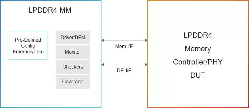
This Cadence® Verification IP (VIP) supports the JEDEC® Low Power Memory Device, LPDDR4 standard. It provides a mature, highly capable compliance verification solution that supports simulation, formal analysis, and hardware acceleration platforms, making it applicable to intellectual property (IP), system-on-chip (SoC), and system-level verification. The LPDDR4 VIP is compatible with the industry-standard Universal Verification Methodology (UVM), runs on all leading simulators, and leverages the industry-standard Cadence Memory Model core architecture, interface, and use model.
The LPDDR4 standard is an industry-leading low power volatile (DRAM) device memory standard for storage of system code, software applications, and user data. LPDDR4 Low Power Memory Device Standard is designed to satisfy the performance and memory density demands of the latest generation of mobile devices such as smart phones, tablets, ultra-thin notebooks, and similar connected devices on the newest, high-speed 4G networks.
Cadence LPDDR4 VIP supports the JEDEC LPDDR4X standard. The LPDDR4X memory saves additional power by reducing the I/O voltage to 0.6V from 1.1V. Other LPDDR4X improvements include a single-channel die option for smaller applications, new MCP, PoP, and IoT packages, and additional definition and timing improvements.
Supported specification: JEDEC JESD209-4C and Refresh management (RFM) and Scaling Parameters.
Key features
- Speed (Mt/s)
- 2133MHz (4266MT/s)
- Device Density
- Supports a wide range of device densities from 4Gb to 32Gb
- Dual Channels
- Supports two channels that can function independently
- General DDR Functionality and Timing Checks
- Precharge, Activate, Read, Write, Mask Write, Mode Register Read, Mode Register Write, Power Down, Refresh, Self Refresh, RFM and related timing checks
- Data Mask and Data Bus Inversion
- Data on the bus can be inverted during both read and write to save power; both Data Mask and Data Bus inversion features can be set through mode registers
- On-the-Fly Burst Length
- Bust length during Read, Write, and Mask Write can be set on the fly through command data and mode registers
- Configurable Preamble and Postamble
- Allows preamble and postamble to be configured for Read, Write, and Mask Write
- Frequency Set Points
- Allows LPDDR4 to be switched between two differing operating frequencies by duplicating mode register parameters commonly changed with operating frequency
- FIFO Register and DQS-DQ Training
- Supports Read FIFO and Write FIFO commands used during Write training
- Multipurpose Command (MPC)
- Supports all 7 MPC commands
- Command Bus Training
- The training centers the internal VREF(ca) in the CA data eye and, at the same time, allows for timing adjustments of the CS and CA signals to meet setup and hold requirements
- Latency Code Frequency Table
- Supports and checks all read and write latency requirements for a given frequency
- Vref Settings
- Supports CA and DQ voltage reference settings
- Single-Ended Mode
- Supports single-ended mode for Clock and Strobe
- Byte Mode
- Supports byte-mode devices from 2Gb to 32Gb
- Tccd+n Reads/Writes
- Supports all combinations of Reads merging and Writes merging placed Tccd+n apart
- Delay Modeling
- Delay modeling of input and output signals, display of delay modeling internal signals on the simulator waveform
- Support for delay randomization on tDQSCK with drifts
Block Diagram
Files
Note: some files may require an NDA depending on provider policy.
Specifications
Identity
Provider
Learn more about LPDDR IP core
LPDDR flash: A memory optimized for automotive systems
A New Generation of LPDDR
SOCAMM: Modernizing Data Center Memory with LPDDR6/5X
On-Device AI Semiconductors & High-speed Interconnects in the Physical AI era
LPDDR6 vs. LPDDR5 and LPDDR5X: What’s the Difference?
Frequently asked questions about LPDDR IP
What is Simulation VIP for LPDDR4?
Simulation VIP for LPDDR4 is a LPDDR IP core from Cadence Design Systems, Inc. listed on Semi IP Hub.
How should engineers evaluate this LPDDR?
Engineers should review the overview, key features, supported foundries and nodes, maturity, deliverables, and provider information before shortlisting this LPDDR IP.
Can this semiconductor IP be compared with similar products?
Yes. Buyers can compare this product with similar semiconductor IP cores or IP families based on category, provider, process options, and structured technical specifications.