Overview
First to market with multiple early adopters of production designs.
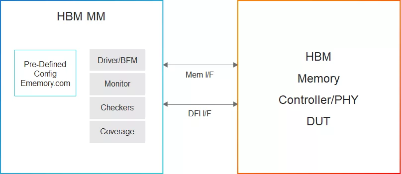
This Cadence® Verification IP (VIP) provides support for the High-Bandwidth Memory (HBM3) interface. It provides a highly capable compliance verification solution applicable to IP, system-on-chip (SoC), and system-level verification. The Cadence Memory Model for HBM3 models a single channel of HBM3 DRAM; this model can be replicated for multiple channels and stacks. The Memory Model for HBM3 runs on all leading simulators, and leverages the industry-standard Cadence Memory Model core architecture, interface, and use model.
The HBM3 DRAM standard is an industry-leading, low-power, double-data-rate, high-data-width, volatile (DRAM) device memory standard for storage of system code, software applications, and user data. The HBM3 DRAM Memory Device Standard is designed to satisfy the performance and memory density demands of the leading-edge high-performance devices.
Supported specification: JEDEC JESD235 Rev 1.27 (HBM), JESD235B Rev 2.50 (HBM2), JESD235B Rev 2.60 (HBM2E), latest HBM3 rev1.0 specification and newer revisions.
Provider

Cadence Design Systems, Inc.
HQ:
USA
If you want to achieve silicon success, let Cadence help you choose the right IP solution and capture its full value in your SoC design. Cadence® IP solutions offer the combined advantages of a high-quality portfolio, an open platform, a modern IP factory approach to quality, and a strong ecosystem.
Now you can tackle IP-to-SoC development in a system context, focus your internal effort on differentiation, and leverage multi-function cores to do more, faster.
The Cadence IP Portfolio includes silicon-proven Tensilica® IP cores, analog PHY interfaces, standards-based IP cores, verification IP cores, and other solutions as well as customization services for current and emerging industry standards. The Cadence IP Factory provides you with an automated approach to the customization, delivery, and verification of SoC IP. As a result, you can spend more time on differentiation, with the assurance that you'll meet your performance, power, and area requirements.
Choosing Cadence IP enables you to design with confidence because you have more freedom to innovate your SoCs with less risk and faster time to market.
Learn more about HBM IP core
LLM inference is increasingly memory-bound, and HBM cost per GB now dominates system cost. Today’s HBM stacks include short on-die ECC, which tightens binning, raises price, and locks reliability policy inside the device. This paper asks a simple question: can we tolerate a much higher raw HBM bit error rate (BER) and still keep end-to-end correctness and throughput, without changing the HBM PHY or the fixed 32B transaction size?
HBM4 is the latest generation of the High Bandwidth Memory (HBM) that has become analogous to the Artificial Intelligence (AI) boom that is everywhere in today’s world. HBM is also increasingly being used in other applications like Data centers, autonomous driving systems, servers, cloud computing just to mention few domains where bandwidth and performance in a key requirement.
High-Bandwidth Memory (HBM) delivers exceptional bandwidth and energy efficiency for AI workloads, but its high cost per bit, driven in part by stringent on-die reliability requirements, poses a growing barrier to scalable deployment. This work explores a systemlevel approach to cost reduction by eliminating on-die ECC and shifting all fault management to the memory controller.
As artificial intelligence (AI) reshapes industries and advances technological frontiers, its success hinges on advanced memory capabilities. Leading this transformation is High Bandwidth Memory (HBM), which offers unparalleled speeds and efficiencies.
In wide chip interfaces like DDR, HBM and ONFI, it can be challenging to synthesize and connect high-frequency controllers to the PHY hard macros. Clock trees can be expansive, pushing tools to their limits, and often multiple clock domains are needed.
With ever increasing need for very high operating frequency of graphics (GPU) or general purpose (CPU) processors, the limited memory bandwidth forms a bottleneck to extract maximum performance out of a system. To add to this, low power consumption, form factor of the memory devices also play significant roles in optimal and efficient solutions.