Generating Chip Subsystems Automatically: A New Answer to Manage Chip Design Complexity

Today’s chips are no longer just processors, they are entire systems. A System-on-Chip (SoC) brings together CPU clusters, accelerators, memories, interconnects and dozens of peripherals, often coming from many different teams and vendors. With AI, high-performance computing and IoT driving demand for ever more capable silicon, the number of blocks, and above all the number of connections between them, keeps growing.
SoCs assembly process is still complex and painful. Connections are listed in spreadsheets and scripts, every IP must be packaged and checked, and any change in the architecture forces design teams to redo a large part of their work. The result is days and sometimes weeks of effort, a heavy reliance on highly specialized skills and rising costs. Design complexity has become a bottleneck for the whole industry.
A new approach: generate SoC subsystems, and simplify the assembly process
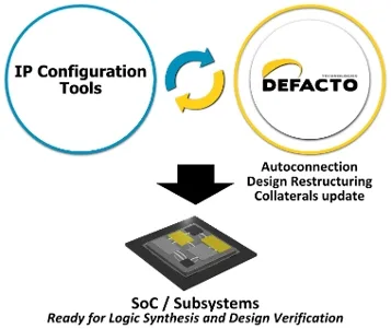
Defacto has just released a new innovation to address this challenge: a solution for SoC subsystem generation. Instead of building a complex SoC from basic IP cores connection by connection, designers describe what they want, and the solution generates first the complete subsystems and afterwards the overall SoC.
Generation means automating the whole creation flow. The solution first reads everything that describes each IPs or building block of the chip: how it connects to the others, how it is powered and what timing it must respect. It then wires the blocks together according to the designer’s intent and finally reorganizes the design to make the chip smaller, faster and more power-efficient.
In the end, it produces all the files that downstream teams need to verify and implement the chip.
Powered by Autoconnection innovation
At the heart of the Defacto new innovation is the Autoconnection capability. In a traditional flow, connectivity is specified explicitly, pairing every driver pin, bus or interface. The Autoconnection replaces this with rules that describe intent. These advanced rules allow the solution to adapt to any type of SoC, whatever its architecture, size or content. The tool derives the detailed connections as a family of rules. The approach can also be driven by AI so that engineers refine a starting point instead of writing everything from scratch. Engineers stay in control since every proposal requires to be reviewed and approved before any subsystem is generated.
Complete support around the generation
Generating a SoC also requires handling all needed design formats and related versions, so Defacto’s innovation brings extended support for the industry’s design RTL and collaterals. This includes the IP-XACT standard to describe IPs, buses and their connectivity, power intent, and timing constraints.
Finally, design restructuring capabilities reorganize the design hierarchy to optimize the chip or meet physical design constraints.
Building SoCs based on the generation of complex subsystems in real projects also means working with basic IP cores the way their providers deliver them. The solution therefore interoperates with the IP configuration tools of the largest IP providers, so that a configured IP flows directly into the generation.
Typical subsystem scenario
The Defacto’ new innovation has been validated by major semiconductor companies to generate HPC, AI and IoT subsystems, showing that it holds across very different SoC architectures. For a typical HPC subsystem with close to a hundred of cores and several hundred of IPs, generating a subsystem takes minutes instead of days and sometimes weeks traditionally.
Changing how chips are designed
The impact of the Defacto new innovation goes beyond building an SoC or a subsystem faster. Designing SoCs faster, with less specialist expertise and at lower cost changes the economics of chip design. It makes much more complex chips achievable, and it opens the door for emerging players to compete with the established semiconductor majors. As chip complexity continues to grow, in particular with the growing demands of AI, methods that scale with the design rather than against it will be essential.
This innovation is co-funded by the European Union through the European Innovation Council (EIC) Accelerator program under Horizon Europe. The project is called EmpoSoC.
Related Semiconductor IP
- I3C Full Controller / Target
- I3C HCI Host Controller
- USB-C Power Delivery IP Core
- Configurable Multi-Channel DMA Controller
- Samsung Foundry 4nm 1V8 GPIO I3C
Related Blogs
- Arasan Chip Systems Inc. Empowers Camera and Display Semiconductor Manufacturers with multiple -Supported Process and Integrated Subsystems, Delivering Cost and Time Savings
- Building Smarter, Faster: How Arm Compute Subsystems Accelerate the Future of Chip Design
- Are IP subsystems the next big IP category?
- IP Roundtable: Subsystems & Software
Latest Blogs
- Generating Chip Subsystems Automatically: A New Answer to Manage Chip Design Complexity
- Agentic AI Should Fit the Way You Engineer
- Listening at the Speed of Memory: Live Speech Recognition on Chimera
- The $725 Million Chip Development: Why Execution Risk, Not IP Cost, Now Dictates Advanced-Node Survival
- From photon to actuation: How physical AI is redefining embedded compute