LPDDR6 Has Arrived ! Innosilicon Technology Delivers LPDDR6 Subsystem IP to Leading Clients
January 21, 2026 -- Recently, Innosilicon Technology, a seasoned player with nearly 20 years of expertise in the IP industry, has announced a major milestone: its self-developed LPDDR6/5X ComboPHY+controller IP has been successfully signed and delivered to a leading industry client. This marks the first commercial collaboration for domestic LPDDR6 interface IP, pioneering commercialization of domestic LPDDR6 interface IP. Innosilicon's LPDDR6/5X Combo IP not only supports multiple generations of advanced FinFET processes but also offers key advantages such as a 14.4Gbps single-line data rate, low power consumption, high bandwidth, low latency, and multi-packaging compatibility. With full generational compatibility, it enables seamless and smooth upgrades from LPDDR5 to LPDDR6. This breakthrough is set to accelerate the commercialization and mass production of the next-generation memory interface technology, offering global chip design companies a high-performance, cost-effective IP solution.
 This commercial signing isn’t coincidental, but built on years of successful cooperation between Innosilicon Technology and its clients, particularly in LPDDR5X/5/4X/4 Combo IPs, delivering excellent PPA (Power, Performance, and Area) results. This landmark collaboration underscores Innosilicon Technology's global competitive edge, technical foundation, and reliability in the high-end DDR series IP sector. Amid the intensifying race for advanced processes in the semiconductor industry, especially with large AI models' extreme dependence on high-speed memory interfaces, high-speed memory IP has become a critical "bridge" connecting the chip's computational core with memory devices. The speed and bandwidth of such interfaces directly impact the token performance and user experience of end products. From DDR3 to MRDDR5, LPDDR2 to LPDDR6, and GDDR7/6X/6 to HBM3E/4, Innosilicon Technology has led the industry by filling key gaps and setting industry standards. Additionally, Innosilicon is currently the world's only IP company that has developed and mass-produced GDDR6/6X and GDDR7.
Following the freezing of the JEDEC LPDDR6 standard in 2024, Innosilicon Technology swiftly delivered to its key clients within just a few months and has been continuously aligning with updates to the JEDEC standards. Innosilicon has made breakthroughs in high-speed, low-power, high-bandwidth, low-latency, and multi-scenario compatibility.
High-Speed
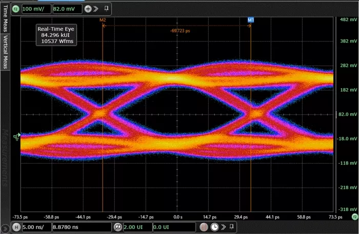
The LPDDR6 IP supports a maximum data rate of 14.4Gbps per data line. This breakthrough stems from Innosilicon’s mature signal processing expertise accumulated from developing high-end storage IPs such as GDDR6X/7 and HBM3E. Through core technologies including customized IO architecture design and full-process optimization of SIPI (Signal Integrity, Power Integrity) simulation, Innosilicon Technology overcame industry challenges such as crosstalk and delay in high-speed transmission at advanced nodes. As a result, the IO speed of the LPDDR6 series was enhanced by 1.5 times, compared to the 9.6Gbps of LPDDR5X, easily meeting the high-bandwidth needs of AI inference and autonomous driving scenarios.
Explore LPDDR6 IP:
High Bandwidth
LPDDR6 represents a revolutionary architectural iteration from 16-bit to 24-bit. To meet the explosive bandwidth demand in fields like AI and HPC, the LPDDR6 standard achieves a dual breakthrough in technical architecture: it not only increases the individual IO rate from LPDDR5X’s typical 9.6Gbps to 14.4Gbps, but it also expands the IO bit width from 8 bits to 12 bits. As a result, the bandwidth of LPDDR6, with a 24-bit 14.4Gbps IO speed per channel, doubles the bandwidth of LPDDR5X with a 16-bit 9.6Gbps IO speed per channel.
Multi-Scenario Compatibility
Innosilicon Technology has integrated advanced IO technologies from the GDDR and LPDDR5/5X series to create a fully compatible LPDDR6/5X Combo IP. Through multiple rounds of IP architecture restructuring and circuit design optimization, Innosilicon has created a solution that ensures the high stability and performance inherent in its DDR series IPs. This solution perfectly aligns with the industry’s "one platform, multi-generation compatibility" development needs, particularly for the large-scale memory compatibility demands brought by AI and HPC applications. This allows a smooth transition from LPDDR5 to LPDDR6 without the need for redeveloping underlying technologies, significantly reducing R&D costs and supply chain risks. Innosilicon’s full compatibility capability has been validated in its DDR5/4 and GDDR7/6 Combo IP products, having empowered the mass production of over 10 billion high-end SoC chips for leading global enterprises.
Top-Tier Process Validation
The rapid commercialization of Innosilicon Technology’s LPDDR6 IP is supported by its full-process node coverage capability and one-stop service system. As one of the few domestic IP vendors supporting process nodes from 55nm to 3nm, Innosilicon Technology has established deep collaborative mechanisms with leading foundries such as TSMC and Samsung to ensure that the LPDDR6 IP is designed with a deep understanding of underlying physical processes, guaranteeing the reliability of the IP.
Moreover, Innosilicon Technology has developed a full-service system covering IP integration simulation, hardening, process parameter customization, and packaging solution design, all supported by a localized technical team. This helps clients reduce their product development cycle by over 30%, enabling them to quickly seize market opportunities.
Facing the digital intelligence era, after nearly 20 years of technical deepening, Innosilicon has established an R&D team of over 1,000 professionals. Its self-developed "high-performance computing IP trio" and full-stack products are empowering LLM applications, supporting scenario customization and SoC integration. This provides quality assurance for accelerating customers' product success while filling gaps in the industry. Currently, Innosilicon's core IP portfolio include the first-to-market LPDDR6/5X, GDDR7/6X, HBM3E/4 Combo, PCIE5/6, UCIE Chiplet, high-speed 112G/224G UALINK, and other high-performance IP products, as well as SoC integration and customization services. These offerings are breaking monopolies and deeply empowering HPC, Auto, and AoT large platform products, helping clients maintain leadership in the high-bandwidth memory field. Innosilicon Technology is committed to becoming the preferred global partner for mass production and delivery to clients worldwide.
Today, Innosilicon Technology has become a core IP partner for numerous leading international clients, with over 10 billion units of advanced process chips shipped. Innosilicon has established an industry-leading “full-cycle closed-loop service system” —a one-stop full-process chain service covering front-end and back-end design, verification, tape-out and mass production, interposer packaging and testing, hardware prototyping, and software driver frameworks. Furthermore, leveraging its LLM system empowerment experience and full-set productization capabilities, Innosilicon assists clients streamline IP integration and software platformization, effectively improving product success rates, shortening development cycles, and continuing to empower clients globally.
Related Semiconductor IP
- LPDDR6 PHY & Controller
- Simulation VIP for LPDDR6
- LPDDR6 Verification IP
- LPDDR6/5X/5 PHY V2 - Intel 18A-P
- LPDDR6/5X/5 Controller IP
Related News
- Innosilicon to Showcase High-Speed Interface IP and Advanced SoC Solutions at the 2025 TSMC OIP Ecosystem Forum
- OPENEDGES Advances Commercialization of LPDDR6/5X Memory Subsystem IP, Targeting Next-Generation AI and HPC Markets
- Innosilicon Announce the world 1st 28nm Litecoin ASIC and Reference Miners
- Innosilicon Receives "Best Partner of the Year 2015" Award from SMIC
Latest News
- EU DARE Project Is Scrambling to Replace Codasip
- Sofics and Alcyon Photonics Partner to Support Next-Generation Photonic Systems
- QuickLogic Appoints Quantum Leap Solutions as Authorized Sales Representative
- Cadence and NVIDIA Expand Partnership to Reinvent Engineering for the Age of AI and Accelerated Computing
- Cadence and Google Collaborate to Scale AI-Driven Chip Design with ChipStack AI Super Agent on Google Cloud