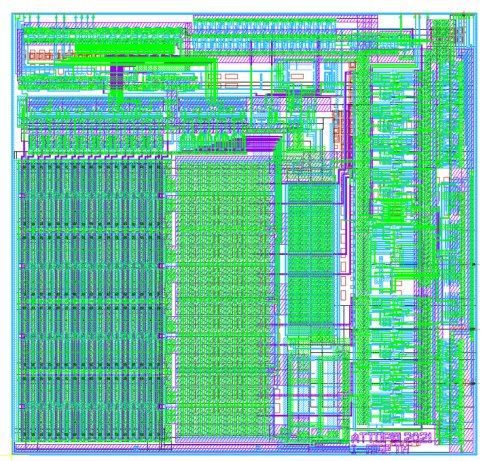
Latest Attopsemi I-fuse OTP Memories Based on Ground-Breaking New Architecture Now Available on X-FAB's 180 nm Technology
Tessenderlo, Belgium and Hsinchu, Taiwan – May 10, 2022 -- X-FAB Silicon Foundries, the leading analog/mixed-signal and specialty foundry, together with Attopsemi, the innovative one-time programmable (OTP) IP solutions provider, today announced that the latest version of Attopsemi‘s I-fuse® IP with its next generation architecture has been successfully demonstrated on X-FAB’s XH018 180 nm process technology. It is available in different memory densities, ranging from 512 bits to 8 KBytes, with several customer projects already being ramped up to volume production.
Attopsemi‘s pioneering new I-fuse S3™ architecture means that the area taken up by the IP is at least 50% less compared to previous versions, without trading off program window range, program voltage and any of the numerous other benefits associated with the original. This enables a dramatic reduction in OTP footprint, as well as a decrease in peak and average current consumption by between 1/3 and 1/2, while still keeping to a 3.3 V standard I/O voltage for programming.
X-FAB’s XH018 is a powerful modular sensor and high-voltage EPI technology, specifically intended for addressing a wide variety of prospective customer scenarios. This technology supports an extended temperature range from -40 to 175°C and a modular 1.8 V/3.3 V ultra-low noise process with a multitude of different automotive-grade non-volatile memory options. Attopsemi’s I-fuse® solution is an optimal fit for X-FAB’s expansive memory portfolio, complementing the company’s current NVM offering. The incorporation of I-fuse® into XH018 will extend the reach of this process into various industrial, medical and consumer applications where 3.3 V operation coupled with compact and cost-effective dies are called for.
“We are pleased with the performance of the XH018. The high reliability of this X-FAB process has resulted in first-time-right integration,” states Shine Chung, Chairman of Attopsemi. “It is very encouraging to see that our collaboration has already triggered new projects with common customers in industrial and consumer areas, and is starting to open up new opportunities throughout the medical sector too.”
“This latest I-fuse® implementation further adds to our successful story of collaboration with Attopsemi. Aligned side-by-side with the present X-FAB proprietary NVM portfolio, the Attopsemi IP solution is broadening the target applications. It presents our customers with an optimized die cost, via the combination of no additional mask layers on top of the XH018 core, plus the footprint reductions that the new architecture enables,” adds Nando Basile, Product Marketing Manager for Memory Solutions at X-FAB. “We now have an increasing number of products where I-fuse® has been embedded, with transitioning to mass production already underway on specific 180 nm and 130 nm platforms.”

About Attopsemi Technology
Attopsemi Technology is a professional OTP intellectual property (IP) provider located in Hsinchu, Taiwan. Since found in 2010, the company has been dedicated to developing and licensing fuse-based OTP IP for all CMOS process, HKMG, FDSOI and FinFET technologies. Attopsemi provides the best possible OTP solutions for all merits in small size, low voltage/current programming/read, high quality, high reliability, low power, high speed, wide temperature and high data security. Attopsemi's proprietary I-fuse™ OTP technologies have been proven in CMOS and other technologies from 0.7 µm to 22 nm in numerous advanced foundries, and has been adopted by many customers in automotive, IoT, and other application fields.
About X-FAB
X-FAB is the leading analog/mixed-signal and MEMS foundry group manufacturing silicon wafers for automotive, industrial, consumer, medical and other applications. Its customers worldwide benefit from the highest quality standards, manufacturing excellence and innovative solutions by using X-FAB’s modular CMOS and SOI processes in geometries ranging from 1.0 µm to 130 nm, and its special silicon carbide and MEMS long-lifetime processes. X-FAB’s analog-digital integrated circuits (mixed-signal ICs), sensors and micro-electro-mechanical systems (MEMS) are manufactured at six production facilities in Germany, France, Malaysia and the U.S. X-FAB employs more than 4,000 people worldwide. www.xfab.com
Related Semiconductor IP
- OTP
- Secure Storage Solution for OTP IP
- GF 22FDX 5.5V OTP Auto-Grade1 IO Staggered
- GF 22FDX 5.5V OTP Auto-Grade1 IO Inline
- NVM OTP XBC TSMC N7 1.8V
Related News
- Eminent Reached 10 Millions of Successful Production Chips Incorporating Attopsemi's I-Fuse OTP
- Attopsemi's I-fuse OTP worked at 0.4V and 1uW read at 22nm process for IoT application
- Attopsemi's I-fuse OTP Passed 250 degrees Celsius for 1,000hrs Wafer-level Burn-in Studies on GLOBALFOUNDRIES 22FDX FD-SOI Technology
- Attopsemi's I-fuse OTP worked at 0.4V and 1uW read on GLOBALFOUNDRIES 22nm FD-SOI for Fraunhofer Institute for Photonic Microsystems' (IPMS) battery-less 61GHz RFID tags
Latest News
- EU DARE Project Is Scrambling to Replace Codasip
- Sofics and Alcyon Photonics Partner to Support Next-Generation Photonic Systems
- QuickLogic Appoints Quantum Leap Solutions as Authorized Sales Representative
- Cadence and NVIDIA Expand Partnership to Reinvent Engineering for the Age of AI and Accelerated Computing
- Cadence and Google Collaborate to Scale AI-Driven Chip Design with ChipStack AI Super Agent on Google Cloud