Installed Capacity for 300mm Wafer Processing Forecast to Rise to 70% of Total Capacity by 2017
Capacity for 200mm wafers forecast to slip more than 10 points during same period.
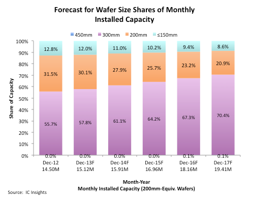
July 03, 2013 -- Since 2008, the majority of integrated circuit production has taken place on 300mm wafers. In terms of surface area shipped (i.e., on a normalized 200mm-equivalent wafer basis), 300mm wafers represented 56% of worldwide installed capacity in December 2012. Production using 300mm wafers is forecast to steadily increase and reach 70.4% in 2017, according to IC Insights’ Global Wafer Capacity 2013 report (see figure).
For the most part, 300mm fabs are, and will continue to be, limited to production of high-volume, commodity-type devices like DRAMs and flash memories, and very recently image sensors and power management devices; complex logic and microcomponent ICs with large die sizes; and products manufactured by foundries, which can fill a 300mm fab by combining wafer orders from many sources.
The list of companies with the most 300mm wafer capacity includes DRAM and flash memory suppliers like Samsung, SK Hynix, Toshiba, Micron, Elpida, and Nanya; the industry’s biggest IC manufacturer and dominant MPU supplier Intel; and two of the world’s largest pure-play foundries TSMC and GlobalFoundries. These companies offer the types of ICs that benefit most from using the largest wafer size available to best amortize the manufacturing cost per die.
It is interesting to point out that when (or if) the pending acquisition of Elpida by Micron goes through as expected, the merged company will have the industry’s second-largest share of 300mm wafer fabrication capacity, trailing only fellow memory chip manufacturer Samsung.
Meanwhile, the share of the industry’s monthly wafer capacity represented by 200mm wafers is expected to drop from 32% in December 2012 to 21% in December 2017, as seen in the figure. Fabs running 200mm wafers will continue to be profitable for many more years and be used to fabricate numerous types of ICs, such as specialty memories, image sensors, display drivers, microcontrollers, analog products, and MEMS-based devices. Such devices are certainly practical in fully depreciated 200mm fabs that were formerly used in making devices now produced on 300mm wafers.

A significant trend with regard to the industry’s IC manufacturing base, and a perhaps worrisome one from the perspective of companies that supply equipment and materials to chip makers, is that as the industry moves IC fabrication onto larger wafers in bigger fabs, the group of IC manufacturers continues to shrink in number. There are about 61% fewer companies that own and operate 300mm wafer fabs than 200mm fabs. The distribution of worldwide 300mm wafer capacity among those manufacturers is very top-heavy. Essentially, there are only about 15 companies that comprise the entire future total available market (TAM) for leading-edge IC fabrication equipment and materials, according to the Global Wafer Capacity 2013 report. When 450mm wafer fabrication technology comes into existence, this manufacturer group is predicted to shrink even further to a maximum of just 10 companies, and a few of those are questionable. Despite growing momentum, IC Insights expects that 450mm wafer capacity will account for only one-tenth of a percent of global IC capacity in December 2017.
Report Details: Global Wafer Capacity 2013
Additional details and a forecast of the IC industry’s wafer fab capacity through 2017 are provided in IC Insights’ Global Wafer Capacity 2013—Detailed Analysis and Forecast of the IC Industry’s Wafer Fab Capacity report. Released in December 2012, the Global Wafer Capacity report assesses the IC industry’s capacity by wafer size, minimum process geometry, technology type, geographic region, and by device type through 2017. The report also includes detailed profiles of the companies most likely to build 450mm wafer fabs and gives detailed specifications on existing wafer fab facilities. Coupled with IC Insights’ Strategic Reviews database of more than 220 company profiles, the two reports provide a tremendous resource for researching, evaluating, and comparing wafer fab facilities and industry capacity. Global Wafer Capacity 2013 is priced at $4,290 for an individual user password. A multi-user worldwide corporate license is available for $6,990.
Related Semiconductor IP
- UCIe D2D Adapter & PHY Integrated IP
- Low Dropout (LDO) Regulator
- 16-Bit xSPI PSRAM PHY
- ASIL B Compliant MIPI CSI-2 CSE2 Security Module
- SHA-256 Secure Hash Algorithm IP Core
Related News
- TSMC's 300mm Chinese Wafer Fab Wins Approval
- Number of 300mm IC Wafer Fabs Expected to Reach 100 in 2016
- Companies Maximizing 300mm, 200mm Wafer Capacity
- IC Makers Maximize 300mm, 200mm Wafer Capacity
Latest News
- TSMC Chases Soaring AI Demand
- EU DARE Project Is Scrambling to Replace Codasip
- Sofics and Alcyon Photonics Partner to Support Next-Generation Photonic Systems
- QuickLogic Appoints Quantum Leap Solutions as Authorized Sales Representative
- Cadence and NVIDIA Expand Partnership to Reinvent Engineering for the Age of AI and Accelerated Computing