Vendor: Silicon Creations Category: Single-Protocol PHY

LVDS interfaces

LVDS-based IOs The Bi-directional LVDS is in production from 90nm CMOS to 16/12nm FinFET and taped out in 7nm FinFET.

TSMC 40nm LP Silicon Proven View all specifications

Overview

LVDS-based IOs

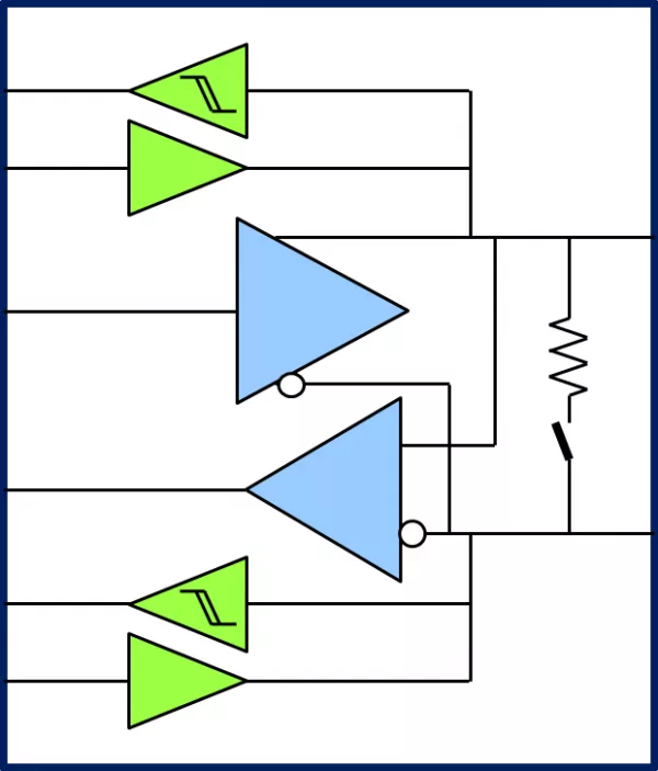
The Bi-directional LVDS is in production from 90nm CMOS to 16/12nm FinFET and taped out in 7nm FinFET. This LVDS I/O is highly programmable and is an excellent IO for FPGA to ASIC conversions.

LVDS-based Interfaces

Based on this versatile LVDS circuit and our robust PLLs and CDR architecture we developed multiple uni-directional and bi-directional parallel source-synchronous interfaces for Chip-chip and Video data transmission. These interfaces can comply with custom chip-chip (or chip-FPGA) requirements or standards including FPDLink, FastLVDS, miniLVDS, FPD Link, Camera Link and OpenLDI.  A dynamic phase alignment and robust word alignment architecture enables data rates exceeding 190Mpixels/s (1.34Gb/s in each lane) for FPD-link and up to 3.3Gbps/lane in some cases. 
Key features

  • Wide operating range
  • High data rates
  • Very flexible programmability
  • Excellent signal integrity
  • TIA/EIA644A LVDS and sub-LVDS compatibility
  • Receiver also compatible with LVPECL
  • Operates over 2Gbps and up to 3Gb/s in some processes
  • Trimmable on-die termination, can be enabled while Tx is operating for better signal integrity
  • Independent LVCMOS input and output functions

Block Diagram

What’s Included?

  • GDSII
  • CDL Netlist (MG Calibre Compatible)
  • Functional Verilog Model
  • Liberty timing models (.lib)
  • LEF
  • Application Note with integration and production test guidelines

Silicon Options

Foundry Node Process Maturity
TSMC 40nm LP Silicon Proven

Specifications

Identity

Part Number
LVDS
Vendor
Silicon Creations
Type
Silicon IP

Files

Note: some files may require an NDA depending on provider policy.

Provider

Learn more about Single-Protocol PHY IP core

The Benefits of a Multi-Protocol PMA

At Silicon Creations, we have developed a power and area optimized, flexible and programmable PMA (Physical Medium Attachment) architecture that can be reliably ported to different process nodes and scaled across protocol generations as data rates increase. It is called the Multi-Protocol PMA, or MP-PMA for short.

Optimized Clocking Solutions for High-Performance Die-to-Die Interfaces

The economics of a system-on-chip ASIC have evolved over the last decade, driven by forces such as cost to yield a transistor, wafer defect density and chip yield, and the drive for greater performance and efficiency. As process nodes continued to shrink from 28nm down to 3nm, we observed Moore’s Law begin to break down, and the cost to yield 100 million transistors normalized to 28nm was either flat or, arguably, increased.

UFS Goes Mainstream

UniversalFlash Storage (UFS) was created for mobile applications and computer systems requiring high performance and low power consumption. These systems typically use embedded Flash based on the JEDEC standard eMMC. UFS was defined by JEDEC as the evolutionary replacement for eMMC offering significantly higher memory bandwidth. The standard builds on existing standards such as the SCSI command set, the MIPI Alliance M-PHY and UniPro as well as eMMC form factors to simplify adoption and development.

Design IP Faster: Introducing the C~ High-Level Language

In this paper, we introduce a new high-level, dataflow programming language called C~ (“C flow”) that further increases productivity by raising the level of abstraction from behavioral descriptions, while overcoming the limitations of C for hardware design. We present the syntax and semantics of this language, and the framework that provides hardware and software code generation. This paper illustrates the benefits of using C~ for hardware design of a IEEE 802.3 MAC, synthesized for FPGA and for 90nm CMOS technology.

Universal Flash Storage: Mobilize Your Data

Universal Flash Storage (UFS) was created for mobile applications and computer systems requiring high performance and low power consumption. These systems typically use embedded Flash based on the JEDEC standard eMMC. UFS was defined by JEDEC as the evolutionary replacement for eMMC offering significantly higher memory bandwidth. The standard builds on existing standards such as the SCSI command set, the MIPI Alliance M-PHY and UniProSM as well as eMMC form factors to simplify adoption and development.

Frequently asked questions about Single-Protocol PHY IP

What is LVDS interfaces?

LVDS interfaces is a Single-Protocol PHY IP core from Silicon Creations listed on Semi IP Hub. It is listed with support for tsmc Silicon Proven.

How should engineers evaluate this Single-Protocol PHY?

Engineers should review the overview, key features, supported foundries and nodes, maturity, deliverables, and provider information before shortlisting this Single-Protocol PHY IP.

Can this semiconductor IP be compared with similar products?

Yes. Buyers can compare this product with similar semiconductor IP cores or IP families based on category, provider, process options, and structured technical specifications.

×
Semiconductor IP