Vendor: IP-Maker Category: NAND Controller

Universal NandFlash Controller

The Universal NAND Flash Controller (IPM-UNFC) IP core is designed specifically to enable commodity Flash memory to be effectivel…

Overview

The Universal NAND Flash Controller (IPM-UNFC) IP core is designed specifically to enable commodity Flash memory to be effectively used in enterprise storage applications requiring high reliability and large interconnect bandwidth. Using the pre-validated IPM-UNFC IP allows greatly reduced time-to-market for storage OEMs desiring higher IOPS benefitting from lower cost SLC, MLC , TLC & QLC NandFlash memory.
 
The IPM-UNFC is full-featured, easy to use in FPGA and SoC designs. For ease of integration with the system interfaces, three native backends (AXI, Avalon and RAM) are provided. The IP core allows page size configuration, spare size per channel.

NandFlash interface

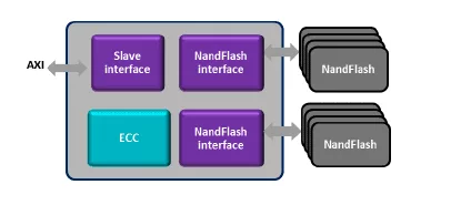
 The NAND flash interface handles all the hardware compliant process (command, address and data sequences). It is ONFI 5.x compliant. Data and Metadata can be protected by the ECC by using configurable data block size (e.g. 1024 bytes + x metadata bytes.) 

Key features

  • ONFI 5.X Compliant
  • SLC / MLC / TLC / QLC
  • SDR modes 0 to 5
  • NVDDR modes 0 to 5
  • NVDDR-2 modes 0 to 8
  • NVDDR-3 modes 0 to 10
  • NV-LPDDR4 modes 0 to 15
  • AXI or Avalon interface
  • Optional DMA interface

Block Diagram

Benefits

  • Cost optimization
  • High performance
  • Reduced Time-To-Market by using validaded IP
  • Full features
  • Simulation testbench

What’s Included?

  • RTL design in verilog.
  • Simulation testbench.
  • Synthesis scripts for Xilinx, Altera and Design Compiler.
  • Documentation.

Specifications

Identity

Part Number
IPM-UNFC
Vendor
IP-Maker
Type
Silicon IP

Files

Note: some files may require an NDA depending on provider policy.

Provider

HQ: France

Learn more about NAND Controller IP core

Re-Use of Verification Environment for Verification of Memory Controller

With the complexity of the design on the rise, coverage of functional verification is one of the increasing challenges faced by the design and the verification teams. Reducing the verification time without compromising the quality of the verification is the greatest challenge to the verification engineers.

The Future of Storage: From eMMC to the Blazing Speeds of UFS 5.0

In the world of mobile and embedded electronics, storage is no longer just about capacity; it’s about how fast that data can move. As we transition into an era of on-device AI and 8K video, the standards we rely on—UFS, eMMC, and NAND—are evolving rapidly.

Building a NAND flash controller with high-level synthesis

In this article, we describe how we were able to apply a commercial HLS tool (Cadence C-to-Silicon Compiler) to a NAND flash controller with an error correction code (ECC) block. The initial ECC design was based on an ECC software program, which led to a large area due to two large arrays. We then used our domain knowledge of the ECC coding theorem to structure the code for hardware implementation.

Frequently asked questions about NAND Controller IP cores

What is Universal NandFlash Controller?

Universal NandFlash Controller is a NAND Controller IP core from IP-Maker listed on Semi IP Hub.

How should engineers evaluate this NAND Controller?

Engineers should review the overview, key features, supported foundries and nodes, maturity, deliverables, and provider information before shortlisting this NAND Controller IP.

Can this semiconductor IP be compared with similar products?

Yes. Buyers can compare this product with similar semiconductor IP cores or IP families based on category, provider, process options, and structured technical specifications.

×
Semiconductor IP