Vendor: VeriSilicon Microelectronics (Shanghai) Co., Ltd. Category: UCIe

Die-to-Die (D2D) Interface for Chiplet Application

Compliant with the UCIe Specification Revision 1.1

Overview

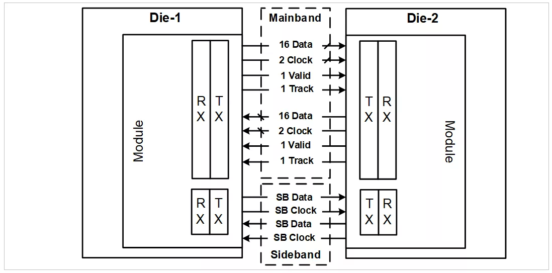
The UCIe PHY IP is a market-leading, ultra low-power, and low-latency interface IP for high-bandwidth connections between two dies that are on the same substrate. The PHY IP implements a wide-parallel and forwarded-clock PHY interface for multi-channel interconnections at data rate up to 24 Gbps per pin.

The PHY IP is configurable to support the leading standards in the industry Universal Chiplet Interconnect Express (UCIe)--providing customers a Die-to-Die (D2D) solution that is compliant with industry standards.


Key features

  • Compliant with the UCIe Specification Revision 1.1
  • Supports 4, 8, 12, 16, and 24 GT/s data rates
  • Self-calibrating and training
  • Supports muti-module (1, 2, or 4) design
  • Sideband channel for initialization and parameter exchange
  • Built-in self-test (BIST), internal loopback, and external PHY-to-PHY link test
  • On-chip calibration for termination impedance
  • Flexible configuration: 16 RX and TX pins per module (standard package)
  • Supports a minimum output driver voltage of 0.5 V
  • Junction temperature range: -40°C to 125°C
  • Package type: standard package
  • Power consumption: < 1.2 pJ/bit @ 16 Gbps (standard package)

Block Diagram

Specifications

Identity

Part Number
UCIe-SP
Vendor
VeriSilicon Microelectronics (Shanghai) Co., Ltd.
Type
Silicon IP
Controller / PHY
PHY

Standards & Interfaces

UCIe Version
UCIe 1.1

Files

Note: some files may require an NDA depending on provider policy.

Provider

Learn more about UCIe IP core

Cadence Silicon Success of UCIe IP on Samsung Foundry’s 5nm Automotive Process

Cadence has successfully demonstrated first-pass silicon success of its UCIe™ standard package IP on Samsung Foundry's 5nm automotive process. This milestone underscores Cadence's commitment to delivering high-performance, automotive-grade IP solutions that meet the stringent requirements of next-generation automotive and high-performance computing applications.

40G UCIe IP Advantages for AI Applications

For AI workloads to be processed reliably at a fast rate, the die-to-die interface in multi-die designs must be robust, low latency, and most importantly high bandwidth. This article outlines the need for 40G UCIe IP in AI data center chips leveraging multi-die designs.

Frequently asked questions about UCIe IP cores

What is Die-to-Die (D2D) Interface for Chiplet Application?

Die-to-Die (D2D) Interface for Chiplet Application is a UCIe IP core from VeriSilicon Microelectronics (Shanghai) Co., Ltd. listed on Semi IP Hub.

How should engineers evaluate this UCIe?

Engineers should review the overview, key features, supported foundries and nodes, maturity, deliverables, and provider information before shortlisting this UCIe IP.

Can this semiconductor IP be compared with similar products?

Yes. Buyers can compare this product with similar semiconductor IP cores or IP families based on category, provider, process options, and structured technical specifications.

×
Semiconductor IP