Overview
Serial Digital Interface (SDI) is the most popular raw video connectivity standard used in television broadcast studios and video production facilities. The availability of high-speed serial inputs/outputs and general purpose programmable logic makes FPGAs (field programmable gate arrays) ideal devices to be used for acquisition, mixing, storage, editing, processing and format conversion applications. Simpler applications use FPGAs to acquire SDI data from one or more SD (standard definition), HD (high definition) or 3G (3-Gigabit HD) sources, perform simple processing and re-transmit the video data in SDI format. Such applications require an SDI PHY (physical layer) interface and some basic processing blocks like a color space converter. In more complex applications, the acquired video is taken through multiple processing phases, like de-interlacing, video format conversion, filtering, scaling, graphics mixing and picture-in-picture display. FPGA devices can also be used as a bridge between SDI video sources and backplane protocols such as PCI Express or Ethernet, with or without any additional video processing.
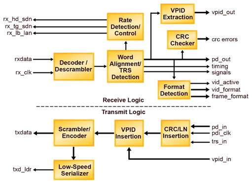
Lattice's Tri-Rate SDI PHY IP (intellectual property) core is a complete SDI PHY interface that connects to the high-speed SDI serial data on one side (through LatticeECP3™ SERDES) and the formatted parallel video data on the other side. It enables faster development of applications for processing, storing, and bridging SDI video data. It is comprised of the following major functional blocks: SDI encoder/decoder, word alignment, CRC detection and checking, VPID (video payload identifier) insertion and extraction, and rate detection logic. The IP core supports the following interface standards and source formats for SDI as specified in standards published by the Society for Motion Picture and Television Engineers (SMPTE).
* Interface: SMPTE 259M-2006 [1] (SD), SMPTE 292M-1998 [2] (HD) and SMPTE 424 M [3] (3G)
* SD source formats: SMPTE 125M [4] and SMPTE 267M [5] (13.5 Mhz only)
* HD source formats: SMPTE 260M [6], SMPTE 274M [7], SMPTE 295M [8] and SMPTE 296M [9]
* 3G source formats: SMPTE 425M [10]
The IP, when connected with the LatticeECP3 SERDES, can transmit and/or receive any of the supported video standards and formats through a common physical serial interface. The IP core can automatically scan and lock on to any of the supported video streams. Receiving multiple standards requires appropriate external clocks to be supplied by the application in response to commands from the IP core.
Learn more about Video Transport IP core
Extending Lattice's post-quantum cryptography leadership from silicon to a complete platform security stack, Lattice Sentry now delivers CNSA 2.0-aligned, NIST-compliant protection across AI data centers, and critical infrastructure, giving system designers a validated, production-ready path to quantum-resistant security.
Combining Arm® AGI CPU server platforms with Lattice FPGAs and AMI firmware creates a solution that provides advanced security, manageability, connectivity, and flexibility for next-generation AI data center infrastructure.
Lattice Prompt pairs with AI agentic tools developers already use, combining them with Lattice design tools, knowledge base, and documentation to turn natural language inputs into validated responses, dramatically accelerating FPGA development while optimizing design performance and capability.
First announced on May 4, 2026, the acquisition creates the industry's most complete secure management and control platform.
The acquisition brings together Lattice’s industry-leading low power FPGAs with AMI’s industry‑leading platform firmware and infrastructure manageability solutions for cloud and AI to create a complete portfolio of secure management and control solutions.
The collaboration demonstrates a real-time AI sensor fusion architecture that integrates TI mmWave radar and camera sensors using NVIDIA Holoscan Sensor Bridge running on Lattice’s low power FPGA. The FPGA acts as a companion chip delivering synchronized sensor data directly into GPU-accessible memory to enable low-latency and robust perception for robotics and industrial edge AI applications.