NPU IP
Silicon-Proven, and Market-Proven IP for Edge AI applications
Overview
GAIA is AIM Future’s scalable Edge AI/ML Inference Accelerator IP Family, built on the company’s proprietary NeuroMosAIc Processor architecture. Based on a single common architecture, the GAIA family scales from less than 64 GOPS to 16 TOPS at 1 GHz, enabling a broad range of edge AI applications from always-on battery-powered sensors and microcontrollers to multi-sensor, multi-modal embedded systems and multi-camera edge computing infrastructure.
At the core of GAIA is a patented, co-developed hardware and software architecture that enables users to efficiently map a single target AI model—or multiple concurrent models—onto the available accelerator resources. This model-to-resource optimization maximizes accelerator utilization, delivering high performance efficiency and industry-leading inference-per-milliWatt efficiency across a wide range of edge AI workloads.
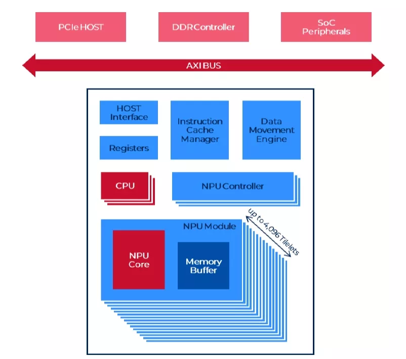
Each GAIA core integrates a Neural Processing Unit (NPU) with a core-local Memory Buffer, supported by shared system resources including a Data Movement Engine, Instruction Cache Manager, NPU Controller, integrated control CPU, Host Interface, and Register Block. The architecture scales to as many as 16, 64, or 256 cores, depending on the GAIA family member, allowing designers to match accelerator performance to specific system requirements.
GAIA is highly configurable by design. MAC arrays and on-chip SRAM can be scaled according to the performance, silicon-area, and power requirements of the target device. This configurability helps avoid over-provisioning of compute and memory resources, while optimizing silicon area and power consumption. For battery-operated and always-on devices, the architecture is designed to maximize the time the processor can remain in deep sleep, further improving overall system energy efficiency.
The GAIA family consists of three performance tiers. GAIA-100 is the smallest and lowest-power member, optimized for sensors, microcontrollers, and low-cost embedded systems. GAIA-200 is the mid-tier member, designed for multi-sensor, multi-modal, and high-end embedded applications. GAIA-300 is the performance-optimized member, targeting multi-camera, multi-modal, and edge computing infrastructure requiring substantially higher AI processing capability.
All GAIA family members share the same Synabro Studio software toolchain, model zoo, and AI framework support. Synabro Studio provides compiler, quantization, and profiling capabilities for AI model development and optimization, with support for TensorFlow/TFLite, ONNX, PyTorch, and Keras front ends. This common software environment enables customers to develop, optimize, and deploy AI models consistently across different GAIA performance tiers.
The parent architecture underlying GAIA has been shipping in production products since 2019, providing a proven foundation for deployment across always-on sensors, high-end embedded systems, and edge computing applications. By combining architectural scalability, configurable compute and memory resources, high accelerator utilization, and energy-efficient operation, the GAIA Series provides a flexible and production-ready AI accelerator IP platform for a wide range of Edge AI SoC designs.
Key features
Scalable Performance & Efficiency
Scales from sub-64 GOPS to 16 TOPS at 1 GHz across the GAIA family. Configurable MAC arrays and on-chip SRAM allow compute, memory, silicon area, and power to be matched to the target device without unnecessary over-provisioning, maximizing performance efficiency and inference-per-milliWatt.
Configurable Multi-Core Architecture
Provides 32 to 8,192 INT8 MACs (8×8) and 8 KB to 8,192 KB of internal SRAM across the family. The architecture scales up to 16 cores for GAIA-100, 64 cores for GAIA-200, and 256 cores for GAIA-300, enabling designers to select the appropriate level of AI compute for each application.
Efficient Core and Data-Movement Architecture
Each core combines a Neural Processing Unit (NPU) with a core-local Memory Buffer, while shared resources—including the Data Movement Engine, Instruction Cache Manager, and NPU Controller—efficiently feed and coordinate processing across multiple cores. This architecture is designed to keep accelerator resources highly utilized while minimizing unnecessary data movement.
Flexible System Integration
An integrated Host Interface, Register Block, and control CPU allow GAIA to be incorporated into a wide range of SoC architectures. GAIA can operate alongside sensors and microcontrollers in low-cost embedded systems, or alongside application processors in multi-sensor, multi-camera, and edge infrastructure SoCs.
INT8 Inference with Transformer Support
All GAIA family members support INT8 inference and Transformer-based workloads, enabling efficient execution of both conventional CNN-based neural networks and emerging transformer-based AI models within edge power and area constraints.
Optional On-Device Training
GAIA-200 and GAIA-300 can be configured with an optional on-device training hardware accelerator engine, enabling on-the-fly model updates and supporting applications that require local adaptation without continuous cloud connectivity.
Production-Ready Software Ecosystem
All GAIA family members share the same Synabro Studio software environment, providing compiler, quantization, and profiling tools together with a model zoo. Supported front ends include TensorFlow / TensorFlow Lite, ONNX, PyTorch, and Keras, enabling a consistent model-development and deployment workflow across the entire GAIA family.
Block Diagram
Benefits
High Energy Efficiency for Edge AI
Industry-leading inference-per-milliWatt efficiency enables efficient AI processing from always-on sensors and battery-powered devices through high-end embedded systems. Configurable compute and memory resources help minimize unnecessary power consumption and maximize deep-sleep residency in power-sensitive designs.
One Scalable Platform Across Multiple Product Tiers
A common NeuroMosAIc Processor architecture, Synabro Studio toolchain, and framework support spans the entire GAIA family, from sub-64 GOPS to 16 TOPS. This allows software development and optimization efforts to be reused across GAIA-100, GAIA-200, and GAIA-300, reducing redevelopment effort as products scale from entry-level to higher-performance applications.
Optimized Silicon Area and Power
Configurable MAC arrays and internal SRAM allow designers to match AI compute and memory resources to the actual requirements of each target device. This helps avoid unnecessary over-provisioning, enabling more efficient use of silicon area and lower power consumption.
Maximum Accelerator Utilization
GAIA’s patented, co-developed hardware and software architecture enables a target model—or multiple models—to be mapped efficiently onto the available accelerator resources. Higher resource utilization improves overall performance efficiency without requiring unnecessarily oversized hardware.
Faster Development and Time to Market
The production-ready Synabro Studio environment provides compiler, quantization, and profiling tools together with a model zoo and support for TensorFlow/TFLite, ONNX, PyTorch, and Keras. A common development environment across the GAIA family helps shorten the path from AI model development to first inference and product deployment.
Greater Edge Autonomy with Optional On-Device Training
GAIA-200 and GAIA-300 can incorporate an optional on-device training hardware accelerator engine, enabling models to be updated locally in the field without requiring continuous connectivity or a cloud round trip. This supports adaptive and cloud-independent edge AI applications.
Reduced Deployment Risk with a Field-Proven Architecture
The parent architecture underlying GAIA has been shipping in production products since 2019. This production history provides customers with a proven technical foundation for integrating GAIA into commercial Edge AI products.
What’s Included?
- Synthesizable RTL of the configured GAIA core, with configuration parameters and integration wrappers.
- Integration and user guide, register specification, and programming model documentation.
- Synthesis constraints and reference scripts, along with power intent files for the target flow.
- Verification environment: testbench, test vectors and regression suite with expected results.
- Synabro Studio software package: compiler, quantizer, profiler, model zoo, runtime and driver.
- FPGA prototyping and bring-up package with reference application examples.
- Release notes, known-issue list and technical support during integration.
Deliverable list is a draft for review; the final package is defined per license agreement and target process.
Specifications
Identity
Provider
Learn more about NPU IP core
AimFuture, a Leader in Home Appliance NPUs, to Integrate Mesacure Company’s AI Algorithms
AimFuture and ITM Semiconductor to Develop AI-Integrated Technology for Robotics and Mobility
ACL Digital and AIM FUTURE Partner to Drive Innovation in Edge AI
AiM Future and Franklin Wireless Sign MOU to Jointly Develop Lightweight AI Model and High-Efficiency 1 TOPS AI SoC Chipset
AiM Future Brings GenAI Applications to Mainstream Consumer Devices
Frequently asked questions about NPU IP cores
What is NPU IP?
NPU IP is a NPU IP core from AiM Future, Inc. listed on Semi IP Hub.
How should engineers evaluate this NPU?
Engineers should review the overview, key features, supported foundries and nodes, maturity, deliverables, and provider information before shortlisting this NPU IP.
Can this semiconductor IP be compared with similar products?
Yes. Buyers can compare this product with similar semiconductor IP cores or IP families based on category, provider, process options, and structured technical specifications.