Vendor: Floadia Corporation Category: Flash

Low Cost SONOS FLASH IP

Cost effective Flash solution up for medium memory capacity requirement up to several 100KBytes

GTA +5 90nm +3 BCD +1 Available on request +3 View all specifications

Overview

LEE Flash G1 (G1) is based on simple SONOS architecture and capable to scale down to 40nm geometry and supports auto grade temperature and quality.

G1 is cost effective Flash solution up for medium memory capacity requirement up to several 100KBytes.

G1 also allows user to re-use IPs and Macros developed for standard CMOS platform because the adoption of G1 process module does not change characteristics of the logic transistors and SPICE model.

Sample Spec

Item Spec
Process platform 180 BCD
Memory Size 256 Kbyte
Word size 64+8
P/E Cycles 100 k
Supply Voltage VDD : 1.62~1.98 V
VCC : 3.0~5.5 V
Additional Masks 2
Operation Temperature(Tj) -40~150 ℃
Data Retention 10years@125℃ post 10K@125℃

High Temperature Operation

SONOS is the device which enables memory functionality trapping electrons in Silicon Nitride film, and the retention life is controlled by optimization of thickness and film properties of oxide and Silicon Nitride films.The data retention characteristics of G1 have been confirmed to be @200°C for more than 10 years.

Large Programming Size enables Short Testing Time

G1 uses FN tunneling technology to achieve extremely low power in program and erase.
It consumes 1/1,000,000 times current, compare to conventional technologies using hot carrier injection for Program/Erase operation.
This also helps reducing testing time, which dominates large portion of the chip cost.

Low Cost

Short Test Time: G1 achieves very short test time for two reasons.

  • Extremely low power in Program/Erase allows tester to Program/Erase the whole memory mat at once, compare to conventional solution Program/Erase smaller sections for many times to Program/Erase the whole memory mat.
  • Sharp Vt distribution in programming will eliminate the requirement for multiple programming and verification, so that programming operation always completes at one time, not in multiple steps, to dramatically reduce programming time.

Short Baking Time

Floadia’s unique memory architecture simplifies Life Time Prediction of the memory cell, which allows chip company to screen devices with shorter baking time.

2-3 Mask adder

G1 requires only 2 to 3 additional masks on standard CMOS process, reducing expensive mask cost to implement NVM feature on your chip. Conventional solution will usually take around 10+ additional masks and uses special manufacturing process.

Re-use of existing IP asset

Unlike normal Flash IPs, our Flash IP does not affect SPICE model of the logic transistors, which means you can utilize existing IPs and assets that has been developed, and will eliminate additional IP investment specific for Flash ICs.
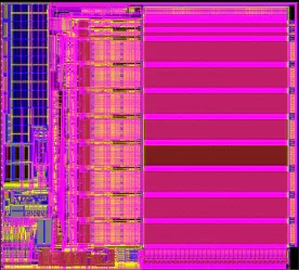

Key features

  • Supports high temperature and long retention life time for severe automotive requirement
  • Low power in Program/Erase operation for power critical applications
  • Requires few (2~3) additional masks
  • No change to SPICE model of Standard CMOS process, for re-using existing design and IP
  • Short Test and Bake time to reduce chip cost

Block Diagram

Silicon Options

Foundry Node Process Maturity
GTA 90nm BCD Pre-Silicon
PSMC 90nm 90nm 900 nm In Production
SK hynix 110nm BCD Available on request
SMIC 90nm BCD Silicon Proven
TSMC 180nm BCDG In Production
Toshiba 130nm 130nm 1300 nm In Production
Toshiba 130nm BCD In Production

Specifications

Identity

Part Number
LEE Flash-G1
Vendor
Floadia Corporation
Type
Silicon IP

Files

Note: some files may require an NDA depending on provider policy.

Provider

Learn more about Flash IP core

Concealable physical unclonable functions using vertical NAND flash memory

Here, the authors propose a concealable PUF using V-NAND flash memory by generating PUF data through weak Gate-Induced-Drain-Leakage (GIDL) erase. The differences in doping depth among V-NAND strings arising from the fabrication cause variations in GIDL erase performance. The resulting V-NAND PUF demonstrated ideal security characteristics while maintaining 100% accuracy under variations in read count and temperature.

Maximizing Performance & Reliability for Flash Applications with Synopsys xSPI Solution

Systems using SoCs designed in advanced processes generally rely on external Flash devices that use NOR/NAND Flash memory technology for non-volatile storage. NOR Flash memory offers many benefits for device manufacturers and consumers, such as faster reading, low power consumption, and smaller area. In contrast, NAND Flash memories are ideal for applications such as data storage, where higher memory capacity and faster write and erase operations are required.

LPDDR flash: A memory optimized for automotive systems

Next-generation automotive systems are advancing beyond the limits of currently available technologies. The addition of advanced driver assistance systems (ADAS) and other advanced features requires greater processing power and increased connectivity throughout the vehicle.

Frequently asked questions about Embedded Flash IP cores

What is Low Cost SONOS FLASH IP?

Low Cost SONOS FLASH IP is a Flash IP core from Floadia Corporation listed on Semi IP Hub. It is listed with support for gta Pre-Silicon; skhynix Available on request; smic Silicon Proven.

How should engineers evaluate this Flash?

Engineers should review the overview, key features, supported foundries and nodes, maturity, deliverables, and provider information before shortlisting this Flash IP.

Can this semiconductor IP be compared with similar products?

Yes. Buyers can compare this product with similar semiconductor IP cores or IP families based on category, provider, process options, and structured technical specifications.

×
Semiconductor IP