Inline memory encryption engine for ASIC SoCs
The IME-IP-341 is an SoC-ready, in-line memory encryption engine using AES/SM4 ciphers with XTS/ECB/Bypass as modes of operation.
Overview
The IME-IP-341 is an SoC-ready, in-line memory encryption engine using AES/SM4 ciphers with XTS/ECB/Bypass as modes of operation. It incorporates multi-stream, multi-algorithm support required for supporting multiple virtual machines (e.g., Realms in ARMv9). It supports configurable protection of different memory regions (up to 32) with separate individual keys mapping to individual regions (e.g., PAS in MPE ARMv9).
The IME-IP-341 provides (optional) protection against power-analysis side-channel attacks by incorporating Differential Power Analysis (DPA) countermeasures within the cipher primitives. Additionally, Datapath Integrity (DI) using ECC based SRAMs with (optional) parity protection in the cipher datapath provides robustness against random errors, ensuring operation under stringent operating conditions in advanced technology nodes. For CMVP certification IME-IP-341 uses a CAVP certified cipher engine and (optional) built in known answer self-test (KAT).
How the IME-IP-341 Engine Works
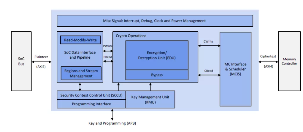
The IME-IP-341 is an inline memory encryption engine for protection of off-chip memory. The programming for the security attributes and keys per region is programmed by a dedicated AMBA interface towards trusted subsystem. At the start, different memory regions (up to 32) can be programmed as per different security policies of the system.
Once the IP is programmed and initialized, it acts as a transparent datapath engine between the SoC bus and DDR controller. It also includes functionality to convert an encryption key into its equivalent decryption. Zeroization, and startup behavior is supported in compliance with MPE engine requirements for ARMv9. The IME-IP-341 supports programmable sector size (default is 64B, same as a typical cache line width and a typical DDR burst size).
Key features
- 128/512-bit (16-byte) encryption and decryption per clock cycle throughput
- Bidirectional design including separate crypto channels for read and write requests, ensuring non-blocking Read
- Read-modify-write supporting narrow burst access.
- Zeroization and support for memory initialization
- Latency: <28 clock cycles for unloaded READ
- AMBA AXI4 complaint 128/512-bit data and 32-bit address channel interface (for Master and Slave integration)
- AMBA APB complaint 32-bit control interface
- Interrupts and internal buffer status flags
- Debug and internal errors
- ECC protection for internal SRAMs
- Zeroization and reset
- CAVP certified AES-XTS crypto core
- FIPS-197, IEEE-P1619/D16, FIPS 140-3 and NIST-SP800-38 standards
Block Diagram
What’s Included?
- Packages
- Documentation
- Tools and scripts
- Integration support
Specifications
Identity
Files
Note: some files may require an NDA depending on provider policy.
Provider
Learn more about Symmetric Crypto IP core
The Post-Quantum Cryptography Mandate: Building Cryptographically Agile Systems for the Quantum Era
Tailoring Root Of Trust Security Capabilities To Specific Customer Needs
Post-Quantum Crypto and Rambus
Rambus IP Solution Supports New NIST Lightweight Cryptography Algorithm
Google, Quantum Attacks, and ECDSA: Why There’s No Need to Panic and Why Preparation Matters Now
Frequently asked questions about Symmetric Cryptography IP cores
What is Inline memory encryption engine for ASIC SoCs?
Inline memory encryption engine for ASIC SoCs is a Symmetric Crypto IP core from Rambus, Inc. listed on Semi IP Hub.
How should engineers evaluate this Symmetric Crypto?
Engineers should review the overview, key features, supported foundries and nodes, maturity, deliverables, and provider information before shortlisting this Symmetric Crypto IP.
Can this semiconductor IP be compared with similar products?
Yes. Buyers can compare this product with similar semiconductor IP cores or IP families based on category, provider, process options, and structured technical specifications.