GCRAM
Provides up-to 50% area reduction and reduced power consumption by a factor ten ive compared to high-density SRAM
Overview
Important industry growth drivers, such as ML, IoT, Automotive and AR/VR, operate on ever-growing amounts of data that is typically stored off-chip in an external DRAM. Unfortunately, off-chip memory accesses are up-to 1000x more costly in latency and power compared to on-chip data movement. This limits the bandwidth and power efficiency of modern systems. In order to reduce these off-chip data movements, almost all SoCs incorporate large amounts of on-chip embedded memory caches that are typically implemented with SRAM and often constitute over 50% of the silicon area. This memory bottleneck is further aggravated since SRAM scaling has reached its limits and no longer shrinks in advanced CMOS process nodes beyond 5nm.
RAAAM™’s patented GCRAM technology provides up-to 50% area reduction and reduced power consumption by a factor ten ive compared to high-density SRAM by utilizing a unique bitcell solution. This enables increasing the on-chip memory capacity using the same die size to provide a dramatic improvement in system bandwidth and power efficiency through reduction or complete removal of off-chip data movement. Alternatively, reducing the memory footprint can lead to substantial fabrication cost savings through die size reduction.
In addition to its area benefits, the GCRAM bit-cell utilizes decoupled write and read ports, providing native two-ported operation at no additional cost, offering a substantial increase in memory bandwidth. Furthermore, GCRAM enables robust voltage scaling capabilities of down to 450mV read and write voltage in 16nm FinFET technology, delivering substantial power savings compared to the foundry and other SRAM solutions.
RAAAM™’s GCRAM technology has already been validated on silicon of leading semiconductor foundries in process nodes ranging from 16nm – 180nm and successfully evaluated in 5nm FinFET technology.
Key features
- Up-to 2X Higher density vs. SRAM
- Up-to 50% area reduction vs. SRAM
- Standard SRAM interface
- Extended interface options vs. SRAM
- Single/two ported
- Up to 2Mbit instances
- Standard CMOS process
- Single cycle operation
- Customizable
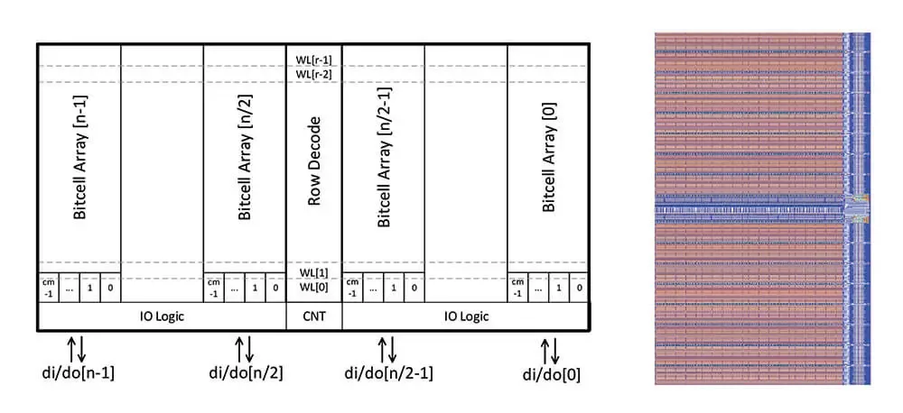
Block Diagram
Benefits
- Extension of Moore’s Law for on chip memories
- Up to 50% Area Reduction vs. SRAM
- Up to 10X Power Reduction vs. SRAM
- Standard CMOS process
Applications
- AI and ML – Weight / Input buffers
- IoT and MCU – System buffers
- Automotive – Large memory caches
- Media Processing – Image / Video buffers
Silicon Options
| Foundry | Node | Process | Maturity |
|---|---|---|---|
| TSMC | 16nm | 16nm 160 nm | — |
Specifications
Identity
Files
Note: some files may require an NDA depending on provider policy.
Provider
Learn more about SRAM IP core
Novel Trade-offs in 5 nm FinFET SRAM Arrays at Extremely Low Temperatures
Why SRAM PUF Technology Is the Bedrock of Dependable Security in Any Chip
AI-driven SRAM demand needs integrated repair and security
A comparison of SRAM vs quantum-derived semiconductor PUFs
Basics of SRAM PUF and how to deploy it for IoT security
Frequently asked questions about SRAM IP cores
What is GCRAM?
GCRAM is a SRAM IP core from RAAAM Memory Technologies Ltd. listed on Semi IP Hub. It is listed with support for tsmc.
How should engineers evaluate this SRAM?
Engineers should review the overview, key features, supported foundries and nodes, maturity, deliverables, and provider information before shortlisting this SRAM IP.
Can this semiconductor IP be compared with similar products?
Yes. Buyers can compare this product with similar semiconductor IP cores or IP families based on category, provider, process options, and structured technical specifications.